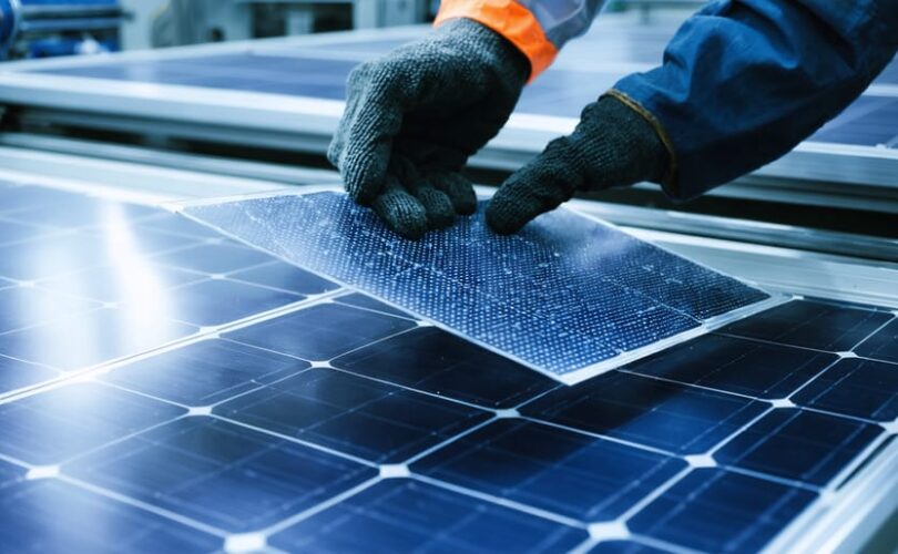
The solar industry faces a defining paradox: photovoltaic technology promises environmental benefits, yet manufacturing solar panels demands significant material resources—silicon, silver, aluminum, copper, and glass—whose extraction and processing carry substantial ecological footprints. As global solar capacity accelerates toward terawatt-scale deployment, the challenge of material efficiency has evolved from an environmental consideration to an economic imperative that directly impacts the industry’s long-term viability and competitive positioning.
Material consumption in solar manufacturing presents three interconnected challenges. First, resource scarcity threatens supply chain stability, particularly for silver conductors and high-purity polysilicon. Second, material costs constitute 60-70% of module manufacturing expenses, creating persistent pressure on profit margins. Third, the environmental burden associated with mining, refining, and transporting these materials contradicts solar energy’s sustainability mission, complicating the complete lifecycle of solar panels.
Recent innovations demonstrate that substantial material reduction is achievable without compromising performance. Silicon wafer thickness has decreased from 180 micrometers to below 130 micrometers in advanced production lines, while silver paste consumption per cell has dropped nearly 80% over the past decade through finer screen-printing techniques and alternative metallization approaches. These achievements, combined with emerging circular economy strategies and next-generation technologies like perovskite-silicon tandems, reveal a clear pathway toward sustainable scaling.
This article examines proven strategies for reducing material consumption across photovoltaic technologies, explores circular economy frameworks reshaping manufacturing practices, and analyzes breakthrough materials poised to redefine solar panel composition. Understanding these developments is essential for professionals navigating an industry where material efficiency increasingly determines both commercial success and environmental credibility.
The Material Challenge in Modern Solar PV Systems
Silicon: The Backbone of Solar Technology
Silicon dominates photovoltaic manufacturing, accounting for approximately 95% of the global solar panel market. This semiconductor material’s unique properties—particularly its ability to convert photons into electrical current—make it indispensable for solar energy generation. However, the journey from raw silica to solar-grade silicon involves an extremely energy-intensive purification process that significantly impacts the environmental footprint of panel production.
The purification process begins with metallurgical-grade silicon (98% pure) and transforms it into polysilicon with 99.9999% purity through chemical refinement. This procedure consumes between 50-100 kWh of energy per kilogram of purified silicon, representing a substantial portion of a solar panel’s total embodied energy. Once purified, manufacturers process this material into either monocrystalline or multi-crystalline wafers, each with distinct material consumption characteristics.
Monocrystalline panels, recognized by their uniform black appearance, require single-crystal silicon ingots grown through the Czochralski process. While they achieve higher efficiency rates (20-22%), this method results in approximately 40-50% material loss during ingot shaping and wafer cutting. Multi-crystalline panels, featuring a distinctive bluish, fragmented appearance, utilize a less wasteful casting process with roughly 30% material loss. Current consumption rates average 4-6 grams of silicon per watt of installed capacity, though continuous technological improvements are steadily reducing these figures through thinner wafers and advanced diamond wire cutting techniques.
Beyond Silicon: Aluminum, Glass, and Silver
While silicon dominates discussions of solar panel materials, the supporting components represent substantial material investments that warrant equal attention in material reduction efforts. Understanding these materials’ footprints is essential for comprehensive sustainability strategies.
**Aluminum frames** account for approximately 10-15% of a solar panel’s total weight. These frames provide structural integrity and mounting support, typically requiring 8-12 kilograms per standard residential panel. The aluminum industry has responded with lighter frame designs and increased use of recycled content—currently averaging 40-60% in solar applications. Some manufacturers now offer frameless designs that eliminate this material entirely while maintaining structural performance through advanced lamination techniques.
**Tempered glass** constitutes the largest mass component, representing 60-70% of panel weight at roughly 10-12 kilograms per panel. Recent innovations have reduced glass thickness from 4mm to 2-2.5mm without compromising protective qualities or durability. This seemingly modest reduction translates to significant material savings across utility-scale installations. Anti-reflective coatings and self-cleaning surface treatments enhance light transmission while reducing maintenance requirements.
**Silver paste** for electrical contacts, though representing less than 0.5% of panel mass, carries disproportionate economic and environmental weight. Silver consumption in photovoltaics exceeds 10% of global silver demand. Manufacturers have reduced silver usage from approximately 100mg per cell in 2016 to 65-75mg today through narrower finger widths and copper-plating alternatives, with targets of 30-50mg per cell by 2030.
**Encapsulation materials**—primarily ethylene-vinyl acetate (EVA) and polyolefin elastomers—protect cells from moisture and mechanical stress. Advanced formulations provide equivalent protection at reduced thickness, while bio-based alternatives emerge from research partnerships between industry and universities, addressing both material efficiency and end-of-life recyclability challenges.
Proven Strategies for Reducing Material Consumption
Thinner Silicon Wafers and Advanced Cutting Technologies
Silicon wafer production has undergone remarkable transformation through advanced cutting technologies that dramatically reduce material waste. Traditional slurry-based wire sawing, which dominated the industry for decades, has been largely replaced by diamond wire sawing technology—a innovation that has revolutionized silicon utilization efficiency.
Diamond wire sawing employs ultra-thin wires embedded with diamond abrasives, achieving kerf loss (material lost during cutting) reductions from approximately 200 micrometers to just 100 micrometers or less. This technological shift alone has decreased silicon waste by nearly 50% during the cutting process. Simultaneously, wafer thickness has decreased substantially from the industry standard of 200-250 micrometers in 2010 to current production thicknesses of 130-160 micrometers, with leading manufacturers achieving wafers as thin as 110 micrometers while maintaining structural integrity.
Kerfless wafer production represents an even more promising advancement, eliminating cutting waste entirely. Technologies such as epitaxial growth, direct wafer formation, and ion implantation lift-off produce wafers without material removal. While still emerging commercially, these methods demonstrate potential silicon savings exceeding 50% compared to conventional sawing techniques.
Universities collaborating on kerfless technology research have documented efficiency improvements and cost reduction trajectories, making these approaches increasingly viable. The combined impact of thinner wafers and advanced cutting methods has reduced silicon consumption per watt of solar capacity by approximately 80% over the past decade, fundamentally reshaping the economics and environmental footprint of photovoltaic manufacturing.
Mono PERC and High-Efficiency Cell Architectures
Passivated Emitter and Rear Cell (PERC) technology represents a significant advancement in reducing material intensity while maximizing solar panel efficiency. This architecture adds a dielectric passivation layer on the rear surface of mono-crystalline silicon cells, which reflects unabsorbed light back into the cell and reduces electron recombination. The result is a conversion efficiency gain of 1-2% absolute compared to standard mono-crystalline cells, translating to more power generated from the same amount of silicon material.
PERC technology achieves efficiencies exceeding 22% in commercial production, with laboratory versions reaching beyond 24%. This improvement means fewer panels are needed to generate equivalent power, directly reducing the silicon, glass, aluminum, and encapsulant materials required per watt of installed capacity. The technology has become industry standard due to its compatibility with existing manufacturing infrastructure and minimal additional processing costs.
Beyond PERC, advanced cell architectures like TOPCon (Tunnel Oxide Passivated Contact) and HJT (Heterojunction Technology) push efficiency boundaries even further, with commercial products achieving 24-25% efficiency. These high-efficiency designs incorporate ultra-thin passivation layers and selective contact structures that extract more energy from each photon absorbed. Universities and research institutions continue collaborating with manufacturers to refine these architectures, driving down the material-to-power ratio through innovative approaches like bifacial configurations and multi-busbar designs that reduce resistive losses while using less silver for metallization.
Alternative Materials and Frameless Designs
The solar industry’s pursuit of material efficiency extends beyond cell architecture to encompass fundamental changes in module construction and component materials. One significant advancement involves replacing silver-based metallization with copper-plated contacts. While silver has dominated solar cell manufacturing due to its excellent conductivity and paste-printing compatibility, its high cost and supply constraints have prompted extensive research into copper alternatives. Copper-plated contacts, protected by appropriate barrier layers to prevent oxidation, offer comparable electrical performance at a fraction of the cost, potentially reducing material expenses by up to 80% for front-side metallization.
Frameless module designs represent another material reduction strategy gaining commercial traction. Traditional aluminum frames, while providing structural support and mounting interfaces, add significant weight and material cost to solar installations. Modern frameless modules utilize enhanced edge sealing and lamination techniques to maintain mechanical integrity without peripheral framing. These designs reduce aluminum consumption by approximately 15-20% per module while facilitating innovative mounting approaches.
Complementing frameless designs, manufacturers have developed thinner glass substrates—reducing thickness from standard 3.2mm to 2.0mm or less—which decrease weight by nearly 40% without compromising durability when properly supported. Lightweight mounting solutions, including polymer-based racking systems and integrated mounting clips, further minimize material intensity. Universities collaborating with industry partners have validated these approaches through accelerated testing protocols, demonstrating that material reduction need not compromise the 25-year performance warranties expected by investors and consumers alike.
Tandem and Multi-Junction Cell Technologies
Multi-junction solar cells represent a breakthrough approach to maximizing energy conversion while minimizing material usage. Perovskite-silicon tandem cells have emerged as particularly promising, combining the high efficiency of crystalline silicon with a thin perovskite top layer that captures different wavelengths of light. This configuration has achieved laboratory efficiencies exceeding 33%, surpassing traditional single-junction limits without substantially increasing material consumption.
The key advantage lies in spectral splitting—each layer absorbs specific light wavelengths most efficiently, reducing energy loss as heat. Research collaborations between universities and industry partners are accelerating commercialization efforts, addressing stability challenges that have historically limited perovskite deployment. Triple-junction cells incorporating additional absorber materials are also under development, though economic viability remains a consideration.
These technologies exemplify how strategic material layering, rather than bulk increases, can dramatically enhance performance. As manufacturing processes mature and educational programs train professionals in these advanced techniques, tandem architectures are positioned to deliver superior efficiency with substantially reduced material intensity compared to conventional approaches.
Material Efficiency Across Different PV Technologies
Monocrystalline vs. Multi-Crystalline Modules
The fundamental difference between monocrystalline and multi-crystalline (also called polycrystalline) silicon modules extends beyond efficiency ratings to encompass significant material consumption variations. Monocrystalline cells, manufactured from single-crystal silicon ingots using the Czochralski process, achieve higher conversion efficiencies of 20-22% but generate substantial material waste during production. The cylindrical ingot cutting process produces approximately 40-50% silicon waste, as manufacturers shape round ingots into square wafers.
Multi-crystalline modules, produced by casting molten silicon into blocks, demonstrate superior material efficiency during manufacturing. This casting process reduces silicon waste to approximately 20-30%, as the rectangular blocks align more closely with the final wafer shape. However, multi-crystalline cells deliver lower conversion efficiencies of 15-17% due to grain boundaries that impede electron flow.
When evaluating performance per gram of silicon, monocrystalline technology increasingly demonstrates advantages. Despite higher production waste, monocrystalline modules generate more power per unit area, requiring less overall material for equivalent energy output in space-constrained installations. Recent technological advances, including diamond wire sawing and thinner wafer production, have reduced kerf loss—the material lost during cutting—from 180 micrometers to under 100 micrometers across both technologies.
The industry trajectory favors monocrystalline modules, which now comprise over 85% of global production. Advanced monocrystalline variants, such as PERC (Passivated Emitter and Rear Cell) technology, achieve efficiencies exceeding 23% while manufacturers continuously refine production processes to recover and recycle silicon waste, improving overall material utilization substantially.
Building-Integrated PV: Solar Tiles and Roof Shingles
Building-integrated photovoltaics (BIPV) represent a paradigm shift in material efficiency by merging construction materials with energy generation capabilities. Solar tiles and roof shingles eliminate the need for separate mounting structures and traditional roofing materials, effectively serving dual purposes while reducing overall material consumption by approximately 30-40% compared to conventional solar installations.
These integrated products replace standard roofing materials entirely, meaning homeowners and builders no longer need to purchase both conventional shingles and separate solar panels. This consolidation significantly decreases the total material footprint across the supply chain, from manufacturing through transportation to installation. Solar tiles typically utilize thin-film photovoltaic technology or miniaturized crystalline silicon cells embedded within durable composite materials that meet building code requirements for weather resistance and structural integrity.
The manufacturing process for BIPV products optimizes material usage by designing photovoltaic components directly into architectural elements. Modern solar shingles incorporate protective layers, semiconductor materials, and structural backing into a single integrated unit approximately 12-15mm thick, compared to traditional systems requiring separate roofing materials plus 40-50mm solar panels with mounting hardware.
Installation efficiency also improves substantially, as roofing contractors can install BIPV products using standard techniques without specialized solar mounting equipment. This reduces both material waste during installation and the carbon footprint associated with multiple trade visits. While BIPV products currently command premium pricing, ongoing research collaborations between manufacturers and universities focus on streamlining production processes to achieve cost parity with conventional approaches while maintaining superior material efficiency.
Circular Economy and Lifecycle Material Management
Solar Panel Recycling Technologies
As photovoltaic installations reach end-of-life, solar panel recycling has emerged as a critical component of sustainable material management. Currently, mechanical and thermal recycling processes can recover up to 95% of materials from crystalline silicon panels, significantly reducing the need for virgin material extraction.
Material recovery rates vary by component: glass comprises 75% of panel weight and achieves recovery rates exceeding 90%, while aluminum frames reach 100% recyclability. Silicon wafers can be recovered at approximately 85% efficiency through specialized processes, though refining them for reuse requires additional energy investment. Precious metals like silver, essential for electrical contacts, present recovery rates of 80-85%, making their reclamation economically attractive given their high market value.
The European Union’s WEEE Directive mandates that producers finance collection and recycling, establishing minimum recovery targets of 85% by weight. This regulatory framework has catalyzed innovation in separation technologies and material purification processes. Similar initiatives are emerging globally, with several U.S. states and Asian countries developing comparable frameworks.
Advanced recycling technologies now employ chemical treatments and high-temperature processes to separate encapsulation materials from cells, enabling higher-purity silicon recovery. These circular economy approaches not only reduce environmental impact but create new revenue streams from recovered materials, effectively closing the loop in solar panel manufacturing while addressing material scarcity concerns for future production scales.

Design for Disassembly and Material Recovery
Manufacturers are increasingly implementing design-for-disassembly principles that facilitate efficient material recovery at end-of-life, creating a circular economy for photovoltaic components. This approach involves using reversible adhesives instead of permanent laminates, modular frame designs with mechanical fasteners rather than welded connections, and standardized component specifications that simplify sorting processes. Leading manufacturers now design modules where aluminum frames, glass, silicon wafers, and copper wiring can be separated with minimal contamination, preserving material quality for reprocessing.
Advanced recycling facilities employ thermal, mechanical, and chemical separation techniques optimized for these new designs, achieving recovery rates exceeding 95% for glass and aluminum, and 85% for silicon and silver. These recycled materials in production reduce dependence on virgin resources while lowering manufacturing energy requirements by up to 30%. Some manufacturers now offer take-back programs, partnering with certified recyclers to ensure proper material recovery. Universities are collaborating with industry partners to develop next-generation separation technologies, including robotic disassembly systems and automated material sorting using AI-based identification, further improving recovery efficiency and economic viability.
Economic and Environmental Benefits of Material Reduction

Cost Reductions and Market Competitiveness
Material efficiency improvements directly impact the economics of solar energy deployment, creating a cascade of cost benefits throughout the value chain. When manufacturers optimize material consumption—whether through thinner silicon wafers, reduced silver paste usage, or lighter frameless designs—they decrease raw material expenses, which constitute 40-60% of total module production costs. These savings translate immediately into lower module prices for installers and consumers.
Beyond manufacturing savings, material reduction significantly improves the levelized cost of energy (LCOE), the metric measuring electricity generation costs over a system’s lifetime. Lighter modules require less structural support and reduced installation labor, cutting balance-of-system expenses by 15-20%. Enhanced material efficiency often correlates with improved conversion efficiency, generating more electricity per installed unit and further reducing LCOE.
These combined cost reductions accelerate grid parity—the point where solar electricity costs match or undercut conventional sources. Markets that achieve grid parity experience exponential growth, as demonstrated by regions where optimized material strategies helped solar become the most economical new electricity source. Educational initiatives from universities and industry collaborations continue advancing material science, ensuring ongoing cost competitiveness while maintaining reliability standards essential for widespread adoption.
Reduced Carbon Footprint and Energy Payback Time
Material reduction in solar photovoltaic technology directly translates to significant environmental benefits. Thinner silicon wafers, advanced thin-film technologies, and optimized module designs require less energy during manufacturing, resulting in a reduced carbon footprint compared to conventional panels. Contemporary crystalline silicon modules now achieve energy payback times of 1-2 years in optimal conditions, while material-efficient thin-film technologies can reach payback periods under one year.
The correlation between material consumption and embodied carbon is substantial. Reducing silicon wafer thickness from 180 to 120 micrometers can decrease embodied energy by approximately 15-20%, while minimizing silver paste usage cuts both material costs and associated carbon emissions. Through comprehensive lifecycle assessment methodologies, researchers have quantified that material-optimized panels produce cleaner electricity throughout their 25-30 year operational lifespan.
Universities partnering with industry leaders continue advancing these metrics through innovative manufacturing processes and material science breakthroughs. This research demonstrates that every gram of material saved multiplies across millions of installed panels, creating measurable planetary-scale environmental improvements while maintaining system reliability and performance standards.
The Road Ahead: Future Innovations in Solar Material Efficiency
The solar industry stands at the threshold of transformative innovations that promise to drastically reduce material consumption while enhancing performance. Emerging research from leading universities and industry laboratories is focusing on several breakthrough technologies that could redefine material efficiency standards in the coming decade.
Perovskite-silicon tandem cells represent one of the most promising frontiers, combining ultra-thin perovskite layers with conventional silicon bases to achieve efficiencies exceeding 30% while using significantly less material. Research collaborations between institutions like MIT, Stanford, and industry partners are addressing stability challenges that have historically limited perovskite commercialization. These partnerships are producing innovative encapsulation techniques and composition modifications that extend operational lifetimes while maintaining minimal material requirements.
Advanced manufacturing techniques, particularly atomic layer deposition and roll-to-roll processing, are enabling precise material application at nanoscale thicknesses. Universities including the National Renewable Energy Laboratory are pioneering these methods, which could reduce silver consumption in solar cells by up to 80% through alternative contact designs and conductive polymers. Industry development priorities increasingly emphasize these ultra-low-material approaches, with several manufacturers targeting commercial deployment within five years.
Artificial intelligence and machine learning are accelerating material discovery processes, analyzing millions of potential compositions to identify candidates that maximize efficiency with minimal resource input. Collaborative platforms connecting academic researchers with industry practitioners are expediting the translation of laboratory discoveries into commercial applications.
The circular economy framework is driving innovation in material recovery technologies, with emerging processes capable of extracting high-purity materials from end-of-life panels at unprecedented efficiency rates. Industry roadmaps now prioritize closed-loop systems where recovered materials feed directly into new panel production, potentially reducing virgin material demand by 40% by 2035.
These innovations, supported by robust educational programs training the next generation of materials scientists and engineers, position the solar industry to achieve unprecedented sustainability while meeting global renewable energy targets.
The imperative to reduce material consumption in solar energy technology extends far beyond cost optimization—it represents a fundamental requirement for achieving truly global sustainability. As photovoltaic installations scale to meet international renewable energy targets, the cumulative demand for silicon, silver, rare earth elements, and other critical materials could strain supply chains and environmental systems. Fortunately, the innovations in material efficiency discussed throughout this article demonstrate that the solar industry is actively addressing these challenges through tangible technological advances.
Efficiency improvements—from high-efficiency silicon cells requiring less material per watt to perovskite tandem architectures maximizing energy capture with minimal resource input—are transforming solar energy from a resource-intensive solution into an increasingly sustainable technology. These material reduction strategies directly translate to lower manufacturing costs, reduced environmental footprints, and enhanced accessibility for developing markets where solar deployment remains critical for energy equity.
For aspiring photovoltaic professionals, this landscape presents exceptional career opportunities. Material science and efficiency optimization have emerged as pivotal disciplines within the renewable energy sector, requiring expertise in semiconductor physics, nanomaterial engineering, manufacturing process innovation, and lifecycle analysis. Professionals who develop competencies in these areas will be instrumental in advancing next-generation photovoltaic technologies and circular economy initiatives.
Educational pathways into this field continue expanding through university partnerships, specialized certification programs, and industry-academic collaborations that provide both theoretical foundations and practical applications. Whether pursuing research roles, manufacturing engineering positions, or sustainability consulting, focusing on material efficiency positions professionals at the forefront of solar energy’s evolution. The convergence of environmental necessity and economic opportunity makes this an exceptionally promising time to contribute to making solar power the cornerstone of global sustainable energy infrastructure.