Solar cells represent a revolutionary breakthrough in photovoltaic systems, transforming sunlight into electrical energy through an elegant dance of physics and materials science. At their core, these sophisticated devices consist of specially treated semiconductor layers that create an electric field when exposed to photons, enabling the efficient harvesting of solar energy. Modern solar cell construction has evolved from simple silicon wafers to complex multi-junction architectures, achieving unprecedented conversion efficiencies exceeding 40% in laboratory conditions. Understanding the intricate relationship between material selection, manufacturing processes, and operational principles is crucial for advancing renewable energy technology and meeting the growing global demand for sustainable power generation. This article delves into the fundamental aspects of solar cell construction and working mechanisms, providing insights into both traditional and cutting-edge fabrication techniques while exploring the physics that makes this remarkable technology possible.
The Basic Structure of a Solar Cell

Silicon Layers and P-N Junction
The fundamental layers of solar cells consist primarily of two distinct silicon layers: the n-type and p-type semiconductors. These layers create the essential p-n junction that enables photovoltaic conversion. The n-type silicon layer is created by doping pure silicon with elements like phosphorus, which introduces extra electrons into the crystal structure. This process creates a negative charge carrier concentration in the material.
Conversely, the p-type silicon layer is formed by doping silicon with elements such as boron, which creates “holes” or positive charge carriers in the crystal lattice. When these two layers are brought together, they form a p-n junction at their interface. This junction creates an electric field due to the diffusion of electrons from the n-type region to the p-type region, and holes moving in the opposite direction.
The resulting depletion region at the junction is crucial for solar cell operation. When photons strike the cell, they excite electrons in the silicon material, creating electron-hole pairs. The electric field at the p-n junction then separates these charge carriers, forcing electrons toward the n-type layer and holes toward the p-type layer. This separation of charges establishes the potential difference necessary for generating electrical current in the solar cell.
Anti-reflective Coating and Metal Contacts
Anti-reflective coatings (ARC) and metal contacts are crucial components that significantly enhance solar cell performance and enable power collection. The ARC is a thin layer applied to the top surface of the solar cell, typically consisting of silicon nitride or titanium dioxide, which minimizes light reflection and maximizes photon absorption. This coating can reduce reflection losses from approximately 30% to less than 5%, substantially improving the cell’s efficiency.
Metal contacts serve as the electrical conduits that collect and transport the generated electrical current. The front contact pattern, usually made of silver, features a grid-like design with thin fingers connected to wider bus bars. This configuration optimizes the balance between electrical conductivity and minimal shading of the cell surface. The rear contact, typically aluminum, covers the entire back surface and forms an electrical contact while also creating a back surface field that reduces electron recombination.
The design and application of these components require precise engineering. The ARC thickness must be carefully controlled to achieve optimal anti-reflective properties for the solar spectrum. Similarly, the metal contact pattern must balance conductivity requirements with minimizing shading losses. Modern manufacturing techniques, such as screen printing and photolithography, enable the precise deposition of these materials while maintaining cost-effectiveness in large-scale production.
The Photovoltaic Effect Explained
Light Absorption Process
The light absorption process in solar cells begins when photons from sunlight strike the silicon material of the cell. When these photons interact with the silicon atoms, they transfer their energy to the electrons in the material’s valence band. If the photon carries sufficient energy – typically 1.1 electron volts (eV) for crystalline silicon – it can excite an electron from the valence band to the conduction band, creating an electron-hole pair.
This process, known as photoelectric effect, is fundamental to photovoltaic energy conversion. Different wavelengths of light carry varying amounts of energy, and silicon solar cells are engineered to optimize absorption across the solar spectrum. The cell’s surface is typically treated with anti-reflective coatings to minimize light reflection and maximize absorption.
The thickness of the silicon layer plays a crucial role in light absorption efficiency. While crystalline silicon requires about 100-200 micrometers to absorb most incoming photons, thin-film technologies utilize special light-trapping techniques to achieve similar absorption in much thinner layers. These techniques include surface texturing and back-reflectors that increase the optical path length of light within the material.
Not all absorbed photons generate usable electricity. Photons with energy below silicon’s bandgap pass through the material without being absorbed, while those with energy significantly above the bandgap lose excess energy as heat through a process called thermalization. Modern solar cell designs incorporate various strategies to minimize these losses and maximize the conversion of absorbed light into electrical energy.

Electron Flow and Electric Current Generation
When light strikes the solar cell, photons interact with the semiconducting material, typically silicon, initiating the photovoltaic effect. This interaction causes electrons in the valence band to absorb enough energy to jump to the conduction band, creating electron-hole pairs. The built-in electric field at the p-n junction drives these freed electrons toward the n-type layer while the holes move toward the p-type layer.
The separation of charge carriers creates an electric potential difference between the front and back contacts of the solar cell. When these contacts are connected through an external circuit, electrons flow from the n-type layer through the circuit to recombine with holes in the p-type layer, generating electric current. This flow of electrons constitutes the electric current that can be harnessed for practical applications.
The efficiency of electron flow depends on several factors, including the quality of the semiconductor material, the design of the p-n junction, and the effectiveness of the electrical contacts. Modern solar cells incorporate various optimization techniques, such as surface texturing and anti-reflection coatings, to maximize photon absorption and electron generation.
The generated current is directly proportional to the intensity of incident light and the active area of the solar cell. Under standard test conditions (STC) of 1000 W/m² irradiance and 25°C cell temperature, a typical silicon solar cell can generate approximately 30-40 milliamperes per square centimeter. This current, combined with the cell’s voltage, determines the overall power output of the solar cell.
Modern Manufacturing Techniques
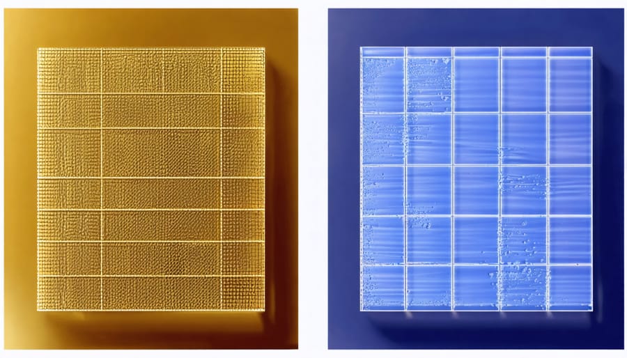
Mono vs Multi-crystalline Production
The production of silicon solar cells primarily follows two distinct crystallization methods: monocrystalline and multicrystalline processing. Monocrystalline silicon is produced using the Czochralski method, where a single crystal seed is dipped into molten silicon and slowly pulled upward while rotating. This process creates a uniform cylindrical ingot with a highly ordered crystalline structure, resulting in higher efficiency solar cells but at a greater manufacturing cost.
In contrast, multicrystalline silicon is manufactured through directional solidification, where molten silicon is poured into a crucible and allowed to cool under controlled conditions. This process creates multiple crystal grains within the silicon block, forming visible boundaries between different crystal orientations. While multicrystalline production is more cost-effective and uses less energy during manufacturing, the resulting solar cells typically achieve lower conversion efficiencies due to electron losses at grain boundaries.
The choice between mono and multicrystalline production methods often depends on specific application requirements and cost considerations. Monocrystalline cells generally achieve efficiencies of 15-22%, while multicrystalline cells typically range from 13-17%. Recent technological advances have narrowed this efficiency gap, making both methods viable options in today’s solar market. Manufacturers must carefully weigh the tradeoffs between production costs, energy consumption, and final cell performance when selecting a crystallization method.
PERC Technology Integration
PERC (Passivated Emitter and Rear Cell) technology represents a significant advancement in solar cell efficiency, offering substantial improvements over traditional solar cell designs. This innovative architecture incorporates additional passivation layers on both the front and rear surfaces of the cell, effectively reducing electron recombination losses.
The key feature of PERC technology is the addition of a dielectric passivation layer on the rear surface, combined with local contact points. This configuration allows sunlight that passes through the cell without being absorbed on the first pass to be reflected back into the cell, providing a second opportunity for absorption and energy conversion.
The passivation layer serves multiple crucial functions: it reduces surface recombination, enhances internal light reflection, and improves the cell’s overall quantum efficiency. Modern PERC cells typically achieve efficiency ratings between 20-23%, representing a significant improvement over conventional cells.
Implementation of PERC technology involves several sophisticated manufacturing processes, including the deposition of aluminum oxide layers, laser ablation for local contact opening, and precise thermal treatment. These processes require advanced equipment and careful control but result in higher energy yields and improved performance under real-world conditions.
The technology has become increasingly standard in commercial solar panel production, offering enhanced performance particularly in low-light conditions and at higher temperatures, making it a preferred choice for both residential and utility-scale installations.
Efficiency Considerations and Future Developments
The efficiency of solar cells remains a critical factor in their commercial viability and widespread adoption. Current commercial solar panel efficiency ratings typically range from 15% to 23%, though laboratory conditions have achieved efficiencies exceeding 40% in multi-junction cells. Several factors influence this efficiency, including material quality, cell design, and environmental conditions.
Material defects and impurities can significantly impact performance by creating recombination centers that reduce electron-hole pair collection. Surface reflection and incomplete absorption of solar radiation also contribute to efficiency losses. Temperature plays a crucial role, with higher temperatures generally decreasing cell efficiency by about 0.5% per degree Celsius above standard testing conditions.
Emerging technologies show promising developments for improving efficiency. Perovskite solar cells have demonstrated rapid efficiency improvements, rising from 3.8% to over 25% in just a decade. Tandem cell architectures, which combine different semiconductor materials to capture a broader spectrum of sunlight, are approaching theoretical efficiency limits of over 45%.
Research focuses on several innovative approaches to enhance performance:
– Advanced light-trapping techniques using nanostructured surfaces
– Novel carrier-selective contacts to minimize recombination losses
– Implementation of quantum dots and other nanomaterials
– Development of transparent conducting oxides with improved electrical properties
Future developments are likely to concentrate on cost-effective manufacturing processes while maintaining high efficiency. Bifacial solar cells, which can capture light from both sides, and building-integrated photovoltaics represent promising directions for maximizing energy yield in real-world applications. These advancements, coupled with ongoing materials research, suggest a trajectory toward both higher efficiency and lower production costs in coming years.
Solar cell technology has evolved significantly since its inception, demonstrating remarkable improvements in efficiency, durability, and cost-effectiveness. Throughout this exploration of solar cell construction and working principles, we’ve seen how the careful selection of materials, precise manufacturing processes, and innovative designs contribute to converting sunlight into usable electricity.
The fundamental components – from the semiconductor layers to anti-reflective coatings and electrical contacts – work in harmony to achieve photovoltaic conversion. Modern manufacturing techniques have enabled the development of various cell types, each optimized for specific applications and environmental conditions.
Looking ahead, the future of solar cell technology appears promising. Emerging technologies like perovskite cells, multi-junction devices, and quantum dot solar cells show potential for pushing efficiency boundaries beyond current limitations. Research continues in areas such as material optimization, alternative semiconductors, and improved manufacturing processes to reduce costs while enhancing performance.
Industry trends suggest continued growth in solar adoption, driven by declining production costs, improved efficiency, and increasing environmental awareness. Advances in energy storage solutions and smart grid integration are addressing intermittency challenges, making solar power increasingly reliable and practical.
As global energy demands rise and environmental concerns persist, solar cell technology remains at the forefront of renewable energy solutions, promising a sustainable path forward for clean energy production.