Advanced photovoltaics represent a quantum leap in solar energy technology, pushing the boundaries of conventional solar cell efficiency and manufacturing processes. Recent breakthroughs in perovskite-silicon tandems have achieved record-breaking conversion efficiencies exceeding 31%, while innovations in multi-junction architectures and novel semiconductor materials are revolutionizing the industry’s potential. These developments, coupled with artificial intelligence-driven manufacturing optimization and quantum dot integration, are transforming photovoltaics from a simple renewable energy source into a sophisticated technological ecosystem.
The convergence of nanotechnology, advanced materials science, and smart manufacturing has catalyzed unprecedented progress in photovoltaic technology. Researchers are now exploring beyond traditional silicon-based cells, incorporating advanced light-trapping mechanisms, surface plasmonics, and innovative electron transport layers to maximize energy harvesting capabilities. These cutting-edge developments promise not only higher efficiency but also reduced production costs and improved durability, making advanced photovoltaics increasingly viable for large-scale commercial deployment.
As the industry evolges toward grid parity and beyond, advanced photovoltaics stand at the forefront of sustainable energy solutions, offering a glimpse into a future where solar power becomes the predominant energy source globally.
Breakthrough Technologies in Modern PV Manufacturing
Mono PERC Innovation
Mono PERC technology represents a significant advancement in photovoltaic cell efficiency through the implementation of passivated emitter and rear contact design. This innovation introduces an additional dielectric passivation layer on the rear side of the solar cell, coupled with local contact points for electrical conductivity.
The manufacturing process involves several sophisticated steps, including the application of aluminum oxide layer through atomic layer deposition, followed by silicon nitride capping and laser ablation to create precise contact openings. This architecture effectively reduces electron recombination at the rear surface while enhancing internal light reflection, resulting in improved photon absorption.
PERC cells demonstrate substantial advantages over traditional aluminum back-surface field (Al-BSF) cells, achieving efficiency gains of 1-2% absolute. Modern PERC manufacturing lines can produce cells with efficiencies exceeding 23% in mass production, while maintaining cost-effectiveness through standardized processes.
Key benefits include:
– Enhanced light absorption through rear surface reflection
– Reduced electron recombination losses
– Improved temperature coefficient performance
– Better low-light performance
– Increased energy yield per installed capacity
The technology’s success has led to rapid industry adoption, with PERC becoming the dominant technology in modern solar manufacturing. Continuous improvements in manufacturing processes and materials have further reduced production costs while maintaining high-quality standards.

Heterojunction Cell Production
Modern heterojunction cell manufacturing represents a significant advancement in photovoltaic technology, combining crystalline silicon with thin-film semiconductor materials to achieve higher conversion efficiencies. The production process involves depositing intrinsic and doped amorphous silicon layers on both sides of a crystalline silicon wafer using plasma-enhanced chemical vapor deposition (PECVD).
Key improvements in manufacturing techniques include the implementation of automated handling systems, precise temperature control during deposition, and advanced surface texturing methods. These refinements have enabled manufacturers to achieve cell efficiencies exceeding 24% in commercial production, with laboratory specimens reaching beyond 26%.
The manufacturing process requires fewer high-temperature steps compared to traditional cell production, resulting in reduced energy consumption and lower thermal stress on the wafers. This advantage translates to fewer breakages and higher yield rates. Advanced quality control systems, incorporating artificial intelligence and machine learning algorithms, monitor the deposition process in real-time, ensuring uniform layer thickness and optimal material properties.
Recent developments in transparent conductive oxide (TCO) application and electrode printing have further enhanced cell performance. Manufacturers now utilize advanced screen-printing techniques and low-temperature silver pastes specifically designed for heterojunction cells, improving conductivity while maintaining the integrity of the temperature-sensitive layers.
Smart Manufacturing Integration
AI-Driven Quality Control
Artificial intelligence has revolutionized quality control in photovoltaic manufacturing, introducing unprecedented precision and efficiency in defect detection. AI-powered quality control systems utilize advanced machine learning algorithms to identify microscopic defects and irregularities that might escape traditional inspection methods.
These systems employ high-resolution imaging and spectral analysis to detect issues such as microcracks, cell misalignment, and material inconsistencies in real-time during production. Deep learning models, trained on vast datasets of defect patterns, can predict potential failure points before they manifest, enabling proactive maintenance and reducing waste.
The implementation of computer vision technology allows for 100% inspection coverage of solar panels, significantly improving upon manual inspection methods that typically sample only a fraction of production output. This comprehensive approach ensures consistent quality across entire production batches while reducing labor costs and human error.
Modern AI systems also integrate with manufacturing execution systems (MES) to provide actionable insights and automated process adjustments. When deviations are detected, the system can automatically fine-tune production parameters or alert operators, maintaining optimal production conditions and ensuring consistently high-quality output.
The result is a marked improvement in overall panel efficiency, durability, and reliability, with defect detection rates exceeding 99% accuracy in many installations. This level of quality assurance is particularly crucial as the industry moves toward more sophisticated cell architectures and advanced materials.
Industry 4.0 Applications
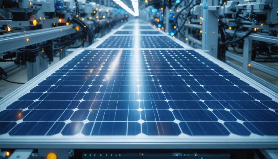
Industry 4.0 principles are revolutionizing photovoltaic manufacturing through the integration of smart technologies and Internet of Things (IoT) systems. Advanced sensors and real-time monitoring systems now enable continuous quality control throughout the production process, significantly reducing defects and improving overall cell efficiency.
Smart manufacturing facilities employ artificial intelligence and machine learning algorithms to optimize production parameters automatically. These systems analyze vast amounts of data from multiple sensors, adjusting variables such as temperature, pressure, and chemical composition in real-time to maintain optimal manufacturing conditions.
Digital twins are increasingly utilized in PV production, creating virtual replicas of manufacturing lines that enable manufacturers to simulate and optimize processes before implementation. This technology reduces setup times and minimizes resource waste while improving product quality.
Automated guided vehicles (AGVs) and robotic systems handle delicate solar cells and materials with precision, reducing breakage rates and increasing throughput. Advanced vision systems and AI-powered quality inspection tools detect microscopic defects that might be missed by human operators.
Cloud-based manufacturing execution systems (MES) provide comprehensive production oversight, enabling remote monitoring and management of multiple facilities. This integration facilitates predictive maintenance, inventory optimization, and enhanced supply chain management.
The implementation of these Industry 4.0 technologies has resulted in significant improvements in production efficiency, with some manufacturers reporting up to 30% reduction in manufacturing costs and 25% increase in throughput rates.
Emerging Materials and Techniques
Perovskite Manufacturing
Perovskite solar technology has revolutionized photovoltaic manufacturing with its promise of high efficiency and cost-effective production methods. The manufacturing process typically involves solution processing techniques, which offer significant advantages over traditional silicon solar cell fabrication.
The primary manufacturing methods include spin coating, blade coating, and slot-die coating. Spin coating, while prevalent in laboratory settings, faces scalability challenges for commercial production. Blade coating and slot-die coating show greater promise for large-scale manufacturing, offering better control over film thickness and uniformity.
A critical aspect of perovskite manufacturing is the precise control of environmental conditions. Temperature, humidity, and atmospheric composition significantly impact crystal formation and film quality. Advanced manufacturing facilities employ specialized environmental chambers and automated processing lines to maintain optimal conditions throughout production.
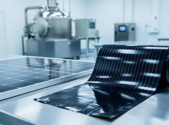
Recent developments in scalable manufacturing techniques have focused on roll-to-roll processing, enabling continuous production of perovskite solar cells on flexible substrates. This approach significantly reduces production costs while maintaining high throughput rates.
Quality control measures include advanced characterization techniques such as X-ray diffraction analysis and scanning electron microscopy to ensure consistent crystal structure and morphology. Manufacturers must also address stability concerns through careful selection of electron and hole transport materials and effective encapsulation strategies.
Tandem Cell Production
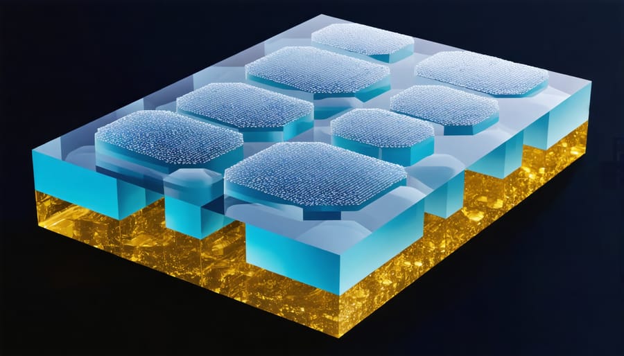
The manufacturing of tandem solar cells represents a sophisticated advancement in photovoltaic technology, combining multiple semiconductor layers to achieve higher conversion efficiencies. The production process begins with the careful deposition of subcells, typically starting with the highest bandgap material at the top and progressing to lower bandgap materials in subsequent layers.
Key manufacturing steps include molecular beam epitaxy (MBE) or metal-organic chemical vapor deposition (MOCVD) for precise layer formation. These techniques enable the growth of crystalline materials with minimal defects, crucial for maintaining high efficiency. The process requires strict control of temperature, pressure, and material composition throughout each layer’s formation.
Tunnel junctions between subcells are created using heavily doped semiconductor materials, allowing efficient charge carrier transport between layers. Advanced monitoring systems ensure optimal interface quality and minimal resistance losses. The incorporation of buffer layers helps manage lattice mismatches between different materials, reducing strain and preventing efficiency-degrading defects.
Modern production facilities employ automated handling systems and real-time quality control measures to maintain consistency across batches. Anti-reflection coatings are applied using plasma-enhanced chemical vapor deposition (PECVD), optimizing light absorption across the solar spectrum. The final steps include metallization for electrical contacts and encapsulation to protect the cell structure from environmental factors.
Quality assurance protocols include spectral response measurements, electroluminescence imaging, and accelerated lifetime testing to ensure long-term performance and reliability.
Advanced Coating Technologies
Advanced coating technologies represent a crucial advancement in modern photovoltaic cell manufacturing, significantly enhancing both performance and durability. Anti-reflective coatings (ARCs) have evolved to achieve remarkable light transmission rates exceeding 99%, maximizing the amount of solar radiation reaching the active layers of photovoltaic cells.
Recent developments include multi-layer nano-structured coatings that combine different materials to optimize performance across the solar spectrum. Silicon nitride remains a standard choice, but new compounds incorporating titanium dioxide and silicon dioxide have shown promising results in laboratory testing, reducing reflection losses by up to 40% compared to conventional coatings.
Protective coatings have also seen significant innovation, with self-cleaning hydrophobic layers that prevent dust accumulation and reduce maintenance requirements. Advanced polymer-based encapsulants provide superior protection against environmental factors while maintaining optimal optical properties. These materials demonstrate enhanced UV stability and moisture resistance, extending panel lifespan beyond 25 years.
Atomic Layer Deposition (ALD) has emerged as a precise coating method, enabling uniform layer deposition at the nanometer scale. This technique allows for precise control over coating thickness and composition, resulting in higher manufacturing consistency and improved cell efficiency.
Current research focuses on developing smart coatings that can adapt to environmental conditions, including thermochromic materials that adjust their properties based on temperature changes, potentially revolutionizing photovoltaic performance in varying climates.
Future Manufacturing Perspectives
The photovoltaic manufacturing landscape is poised for significant transformation over the next decade, driven by technological advancements and increasing demand for more efficient solar solutions. Industry experts anticipate that artificial intelligence and machine learning will play pivotal roles in optimizing production processes, reducing waste, and improving quality control mechanisms.
Perovskite-silicon tandem cell manufacturing is expected to emerge as a mainstream technology, with several major manufacturers already investing in pilot production lines. These cells promise to break the 30% efficiency barrier while maintaining cost-effectiveness through streamlined manufacturing processes.
Advanced automation and robotics will likely revolutionize production lines, enabling 24/7 operations with minimal human intervention. This shift towards Industry 4.0 principles will incorporate real-time monitoring systems, predictive maintenance, and digital twins to ensure optimal production efficiency.
Sustainable manufacturing practices will become increasingly important, with manufacturers focusing on reducing carbon footprints through renewable energy use in production facilities and implementing circular economy principles. This includes developing better recycling processes for end-of-life panels and utilizing recycled materials in new panel production.
Building-integrated photovoltaics (BIPV) manufacturing is expected to see substantial growth, requiring new production techniques and materials to meet architectural specifications while maintaining high energy conversion efficiency. Additionally, flexible and lightweight solar panel manufacturing will likely expand to serve emerging markets such as electric vehicles and portable electronics.
The industry is also moving towards more localized production facilities to reduce transportation costs and carbon emissions, with several regions developing manufacturing hubs supported by robust supply chains and skilled workforce development programs.
The evolution of advanced photovoltaics continues to reshape the renewable energy landscape through innovative manufacturing processes and breakthrough technologies. As we’ve explored, smart manufacturing integration, novel materials, and automated quality control systems are driving unprecedented improvements in solar cell efficiency and production costs. The industry’s commitment to sustainability is evident in the adoption of circular manufacturing practices and the development of more environmentally friendly production methods.
Looking ahead, the future of advanced photovoltaic manufacturing appears promising, with several key trends poised to drive further innovation. Artificial intelligence and machine learning will play increasingly crucial roles in optimizing production processes, while emerging technologies like perovskite solar cells and tandem devices show potential for revolutionary efficiency gains. The integration of Industry 4.0 principles is expected to enhance manufacturing precision and reduce operational costs significantly.
As global demand for renewable energy solutions continues to grow, investments in research and development will accelerate technological advancement. Collaboration between industry leaders, research institutions, and technology providers will be crucial in overcoming current limitations and pushing the boundaries of photovoltaic efficiency and sustainability.