
The solar industry stands at a pivotal crossroads as perovskite solar cells emerge to challenge silicon’s four-decade dominance of the photovoltaic market. Silicon currently commands over 95% of global solar installations, yet perovskite technology has achieved a remarkable efficiency leap from 3.8% to over 26% in just fifteen years—a progression that took silicon nearly half a century. This unprecedented advancement has sparked intense debate among researchers, manufacturers, and investors about whether perovskites represent an evolutionary improvement or a revolutionary replacement for conventional silicon panels.
Understanding the distinctions between these technologies requires examining their fundamental material properties, manufacturing processes, performance characteristics, and commercial readiness. Silicon offers proven durability with 25-30 year warranties and established supply chains, while perovskites promise lower production costs, superior low-light performance, and flexible form factors that could unlock entirely new applications. However, perovskites face critical challenges in stability, scalability, and lead content that currently prevent widespread deployment.
This comprehensive analysis evaluates both technologies across efficiency metrics, degradation rates, manufacturing economics, environmental impact, and market positioning. Rather than positioning this as a binary competition, the evidence suggests a more nuanced future where perovskite-silicon tandem cells, pure perovskite modules for specialized applications, and continued silicon refinements will likely coexist, each serving distinct market segments based on performance requirements and cost considerations.

Understanding Silicon Solar Cells: The Industry Standard
How Silicon Solar Cells Work
Silicon solar cells have dominated the photovoltaic industry for decades, establishing themselves as the benchmark technology for solar energy conversion. These cells operate on the photovoltaic effect, where semiconductor materials convert sunlight directly into electricity through a carefully engineered process.
At their core, silicon solar cells consist of two layers of silicon that have been chemically modified through a process called doping. The top layer is doped with phosphorus to create an abundance of electrons (n-type), while the bottom layer is doped with boron to create electron deficiencies or “holes” (p-type). When these layers meet, they form a p-n junction, creating an electric field at the boundary.
When sunlight strikes the cell, photons transfer their energy to electrons in the silicon atoms, freeing them from their atomic bonds. The electric field at the p-n junction drives these freed electrons toward the n-type layer and holes toward the p-type layer, creating a flow of electrical current. Metal contacts on the top and bottom of the cell collect this current for external use.
The industry primarily utilizes two variants: monocrystalline and multi-crystalline technologies. Monocrystalline cells, manufactured from single silicon crystals, offer higher efficiency rates of 20-22% due to their uniform crystal structure that allows electrons to flow more freely. Multi-crystalline cells, made from multiple silicon fragments melted together, provide a more cost-effective option with slightly lower efficiencies of 15-18%. Both technologies have proven reliability, with performance warranties typically extending 25-30 years, making them the trusted foundation of modern solar installations worldwide.
Silicon’s Proven Track Record
Silicon solar cells have dominated the photovoltaic industry for over six decades, establishing an unmatched track record that continues to define commercial solar deployment. This dominance stems from a mature manufacturing ecosystem with proven scalability, enabling mass production at competitive costs. Global manufacturing infrastructure supports annual production capacities exceeding 200 gigawatts, with established supply chains spanning raw material processing to module assembly.
The reliability of crystalline silicon technology represents perhaps its most compelling advantage. Modern silicon panels typically carry 25 to 30-year performance warranties, with many installations exceeding these timeframes while maintaining over 80% of their original efficiency. Field data from systems operating since the 1980s demonstrates silicon’s exceptional durability across diverse climatic conditions, from desert heat to arctic cold.
Performance stability under real-world conditions further distinguishes silicon technology. Unlike emerging alternatives, silicon cells exhibit minimal degradation from moisture, heat, and UV exposure when properly encapsulated. This predictable performance allows accurate long-term energy yield modeling, critical for project financing and return-on-investment calculations. Universities collaborating with industry partners continue refining silicon cell architectures, recently achieving laboratory efficiencies approaching 27% for single-junction designs, demonstrating that this established technology still holds innovation potential.
What Makes Perovskite Solar Cells Different
The Perovskite Crystal Structure
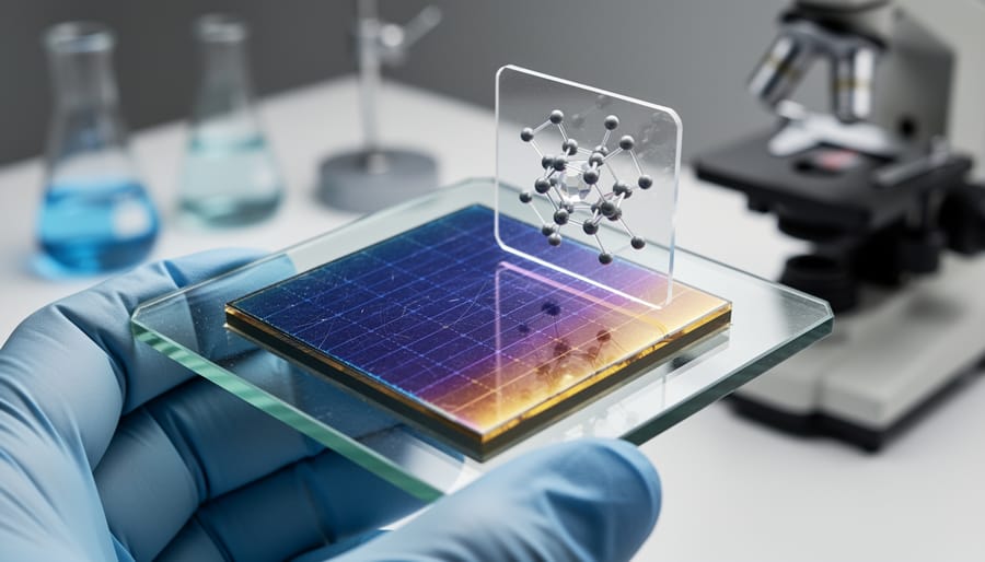
Perovskite solar cells derive their name from the distinctive crystal structure they share with the mineral perovskite (calcium titanium oxide). The most commonly studied photovoltaic perovskites are hybrid perovskites, typically methylammonium lead halide compounds with the chemical formula CH3NH3PbX3, where X represents a halogen ion such as iodide, bromide, or chloride.
The perovskite crystal structure follows an ABX3 arrangement, where the larger organic cation (A) occupies the corners of a cubic lattice, lead atoms (B) sit at the center, and halide ions (X) form an octahedral cage around the lead. This unique architecture creates exceptional optoelectronic properties that make perovskites remarkably effective at converting sunlight into electricity.
What distinguishes perovskites from conventional silicon is their direct bandgap, which enables efficient light absorption across a broad spectrum of wavelengths. Perovskite materials can absorb significantly more light per unit thickness compared to silicon, requiring layers only 300-500 nanometers thick versus silicon’s 180 micrometers. This direct bandgap also facilitates rapid charge carrier generation and transport, minimizing energy losses.
Additionally, perovskite materials exhibit tunable bandgaps through compositional modifications, allowing researchers to optimize absorption characteristics for specific applications. Their high absorption coefficient, long carrier diffusion lengths, and low exciton binding energy contribute to rapid efficiency improvements that have captivated the photovoltaic research community and industry stakeholders worldwide.
Manufacturing Process: Simpler and Cheaper
The manufacturing advantages of perovskite solar cells represent one of their most compelling attributes when compared to traditional silicon technology. Silicon solar cells require energy-intensive production processes involving temperatures exceeding 1,400°C to purify silicon and form crystalline wafers. This high-temperature fabrication consumes substantial amounts of electricity and necessitates specialized, expensive equipment, contributing significantly to both production costs and the technology’s carbon footprint during manufacturing.
In stark contrast, perovskite solar cells can be manufactured through solution processing techniques at temperatures typically below 150°C, and in some cases even at room temperature. The perovskite material is dissolved in a solvent and then applied to substrates using methods such as spin coating, blade coating, slot-die coating, or inkjet printing. These techniques are fundamentally simpler and more compatible with roll-to-roll manufacturing processes similar to newspaper printing, enabling rapid, large-scale production.
This low-temperature approach dramatically reduces energy consumption during manufacturing, potentially cutting production costs by up to 50% compared to silicon. The reduced equipment complexity and lower capital expenditure requirements make perovskite manufacturing more accessible, potentially democratizing solar panel production. Universities collaborating on perovskite research have demonstrated laboratory-scale manufacturing processes that could transition to commercial production more readily than silicon alternatives.
However, scaling these solution-based processes while maintaining consistent quality and long-term stability remains an ongoing challenge that researchers and manufacturers continue to address through improved deposition techniques and quality control measures.
Head-to-Head Performance Comparison
Efficiency: Closing the Gap Rapidly
Power conversion efficiency remains a critical metric for evaluating solar cell technologies. Silicon solar cells currently lead commercial production with laboratory efficiencies reaching 26-27%, representing the culmination of nearly 70 years of intensive research and development. However, perovskite solar cells have demonstrated remarkable progress, achieving certified efficiencies exceeding 25% in just over a decade of focused development since 2009.
This accelerated improvement trajectory positions perovskites as one of the fastest-advancing photovoltaic technologies in history. Silicon technology improved gradually over decades, requiring substantial investment in materials science, manufacturing processes, and device architecture. In contrast, perovskites have closed this efficiency gap through rapid optimization of composition, interface engineering, and deposition techniques.
The narrowing performance difference suggests perovskites may soon match or surpass silicon in laboratory settings. Furthermore, tandem configurations combining perovskite and silicon layers have already achieved efficiencies above 33%, exceeding the theoretical limit of single-junction silicon cells. These developments demonstrate significant potential for next-generation solar technology, though translating laboratory results into commercially viable products remains an ongoing challenge requiring collaboration between research institutions and industry partners.
Cost and Manufacturing Economics
Manufacturing economics present a compelling distinction between these technologies. Silicon solar cells require energy-intensive production processes, including purification at temperatures exceeding 1400°C and complex crystal growth techniques. The capital expenditure for silicon manufacturing facilities typically ranges from $200-500 million, creating significant barriers to market entry.
Perovskite solar cells offer transformative cost advantages through solution-based processing at temperatures below 150°C. This low-temperature fabrication enables compatibility with flexible substrates and roll-to-roll manufacturing techniques, potentially reducing production costs by 50-70% compared to crystalline silicon. Material expenses further favor perovskites, as their thin-film architecture requires only micron-scale layers versus the 180-200 micrometer thickness of silicon wafers.
Current silicon module costs have declined to approximately $0.20-0.30 per watt, setting a competitive benchmark. Industry analysts project perovskite modules could achieve costs below $0.15 per watt at scale, though this remains theoretical pending commercial validation. The scalability equation also involves coating uniformity challenges and materials supply chains that require development. Universities collaborating with industry partners are actively researching manufacturing optimization, while educational programs train the next generation of professionals in these emerging production methodologies, accelerating the pathway toward cost-competitive perovskite manufacturing.
Durability and Lifespan
Silicon solar cells have established an impressive track record with operational lifespans routinely exceeding 25-30 years, backed by decades of field data and standardized testing protocols. Manufacturers typically guarantee 80-90% power output after 25 years, demonstrating crystalline silicon’s remarkable stability under real-world conditions.
Perovskite solar cells, conversely, face significant durability challenges that currently limit their commercial viability. The primary concern involves moisture sensitivity—perovskite materials degrade rapidly when exposed to water vapor, requiring robust encapsulation strategies. Thermal instability presents another critical issue, as elevated temperatures can trigger phase transitions and material decomposition. Additionally, prolonged UV exposure accelerates degradation through photochemical reactions within the perovskite layer.
Recent research has made substantial progress addressing these stability concerns. Advanced encapsulation techniques, compositional engineering with mixed-cation formulations, and protective interfacial layers have extended laboratory lifespans from mere hours to over 10,000 hours under accelerated testing conditions. However, achieving the 25-year threshold demanded by the solar industry remains a formidable challenge. Universities and research institutions continue developing innovative stability enhancement strategies, while educational programs are training the next generation of professionals to tackle these durability limitations. Until perovskites demonstrate long-term outdoor reliability matching silicon’s proven performance, widespread deployment will remain constrained.
Flexibility and Application Versatility
Perovskite solar cells offer remarkable versatility compared to traditional silicon panels. Their solution-based manufacturing process enables deposition on flexible substrates like plastics and thin films, making them ideal for flexible solar applications including building-integrated photovoltaics, curved surfaces, and wearable electronics. With thicknesses below 1 micrometer versus silicon’s 180-200 micrometers, perovskites provide lightweight solutions weighing significantly less than conventional modules. Additionally, perovskite cells can be tuned for semi-transparency, opening opportunities for solar windows and architectural glazing. Silicon, conversely, remains confined to rigid, opaque panel configurations due to its crystalline structure and manufacturing requirements. While silicon’s established infrastructure excels in utility-scale ground-mounted installations, perovskites promise to unlock entirely new market segments where weight, flexibility, and aesthetics are paramount considerations for deployment.
Environmental Impact and Sustainability
Silicon solar cells require energy-intensive manufacturing processes, including polysilicon purification at temperatures exceeding 1,400°C, contributing significantly to their environmental impact. Perovskite cells promise lower manufacturing energy requirements through solution-based processing at near-room temperatures, potentially reducing carbon footprint by up to 40%.
However, perovskites face scrutiny over lead content, with most high-efficiency formulations containing this toxic element. While encapsulation can mitigate immediate risks, end-of-life disposal and potential environmental contamination remain concerns. Research into lead-free alternatives continues, though performance currently lags behind lead-based versions.
Silicon panels benefit from established recycling infrastructure, recovering up to 95% of materials including glass, aluminum, and silicon. Perovskite recycling frameworks remain underdeveloped, though their simpler composition may eventually facilitate material recovery. Universities and industry partners are collaborating on sustainable perovskite designs and circular economy solutions to address these environmental challenges before large-scale commercialization.
The Tandem Cell Solution: Best of Both Worlds
How Tandem Cells Work
Tandem solar cells represent a breakthrough approach that combines the complementary strengths of perovskite and silicon technologies. In this configuration, a thin perovskite layer is deposited on top of a conventional silicon cell, creating a two-junction device that captures a broader spectrum of sunlight more efficiently than either material alone.
The physics behind tandem cells is elegant: perovskite materials excel at absorbing high-energy blue and green photons from the visible light spectrum, while silicon efficiently captures lower-energy red and near-infrared wavelengths. By stacking these layers strategically, the perovskite top cell harvests shorter wavelengths first, then allows longer wavelengths to pass through to the silicon bottom cell. This spectral splitting minimizes thermalization losses that occur when single-junction cells convert high-energy photons, a fundamental limitation described by the Shockley-Queisser limit.
Laboratory demonstrations have already achieved certified efficiencies exceeding 33 percent, surpassing the theoretical maximum of approximately 29 percent for single-junction silicon cells. Research institutions collaborating with universities worldwide continue pushing these boundaries, with some projecting potential efficiencies approaching 35 percent. This substantial performance gain makes tandem technology particularly attractive for space-constrained installations where maximizing power output per unit area is critical.

Commercial Viability of Tandem Technology
Tandem perovskite-silicon technology has progressed significantly from laboratory demonstrations to pre-commercial stages. Several companies worldwide are actively developing these hybrid cells for market introduction. Oxford PV, a spin-off from the University of Oxford, leads commercialization efforts and has established manufacturing facilities in Germany, targeting initial production of tandem modules with efficiencies exceeding 26%. Polish manufacturer Saule Technologies and Swiss company Insolight are also advancing tandem cell production capabilities.
Current industry projections suggest limited commercial availability could begin within 2-3 years, primarily targeting premium applications where higher efficiency justifies increased costs. However, widespread market adoption faces substantial hurdles including manufacturing scale-up, long-term reliability validation under diverse environmental conditions, and cost reduction to competitive levels. Most analysts anticipate tandem cells will initially serve niche markets such as space-constrained rooftop installations and building-integrated photovoltaics before potentially expanding to utility-scale projects.
Research partnerships between manufacturers and universities continue accelerating development, with institutions offering specialized training programs to prepare the workforce for this emerging technology. The transition from laboratory achievements to commercial success ultimately depends on demonstrating 25-30 year operational lifetimes while maintaining manufacturing costs within acceptable margins.
Current Market Reality and Commercialization Challenges
The Stability Problem
The primary barrier preventing perovskite solar cells from reaching widespread commercialization remains their susceptibility to degradation. Unlike silicon cells that maintain performance for 25-30 years, perovskite materials deteriorate when exposed to moisture, oxygen, ultraviolet radiation, and elevated temperatures. This instability stems from the crystalline structure’s sensitivity to environmental stressors, causing rapid efficiency losses that currently limit operational lifespans to months rather than decades.
Research institutions worldwide, including collaborations with leading universities, are developing multifaceted solutions to address these degradation mechanisms. Current strategies include engineering moisture-resistant encapsulation layers using advanced polymers and glass composites, incorporating hydrophobic additives into the perovskite formulation, and developing two-dimensional perovskite structures with enhanced stability. Researchers have also achieved promising results by replacing volatile organic components with more stable alternatives and creating hybrid structures that combine perovskites with protective oxide layers.
Recent breakthroughs demonstrate accelerated aging tests showing certain perovskite formulations maintaining over 90 percent efficiency after 1,000 hours of continuous operation under controlled conditions. While significant progress continues, achieving the industry-standard 25-year warranty threshold remains an ongoing challenge. Educational programs focused on materials science and photovoltaic engineering are preparing the next generation of researchers to tackle these durability challenges systematically.

Scaling from Lab to Factory
Scaling perovskite solar cells from laboratory to commercial production presents significant technical challenges that silicon technology has already mastered over decades. While researchers routinely achieve record efficiencies with small perovskite cells measuring less than 1 cm², maintaining these performance levels across large-area modules of 1 m² or more proves problematic. Uniform deposition of perovskite films becomes increasingly difficult at scale, leading to defects and performance variations across the panel surface.
Silicon manufacturing benefits from well-established automated processes and quality control systems developed through years of industrial refinement. In contrast, perovskite production methods like spin-coating work excellently in laboratories but are unsuitable for mass manufacturing. Emerging techniques such as slot-die coating and vapor deposition show promise for large-scale production, yet these processes require substantial optimization to achieve commercial viability.
The transition also reveals material stability issues that become more pronounced in larger installations. Temperature gradients, moisture ingress at edges, and mechanical stress during handling all impact performance consistency. Universities and research institutions are actively collaborating with industry partners to develop scalable manufacturing protocols, with several pilot production lines now operational worldwide testing various deposition techniques and encapsulation strategies.
Regulatory and Safety Considerations
A primary concern surrounding perovskite solar cells involves their lead content, which poses potential environmental and health risks if cells are damaged or improperly disposed of. Unlike silicon cells, which contain minimal toxic materials, most high-efficiency perovskite formulations rely on lead-based compounds. Regulatory frameworks in many jurisdictions restrict lead usage in consumer products, creating potential barriers to widespread commercialization.
The photovoltaic research community is actively addressing these concerns through two parallel approaches. First, scientists are developing lead-free perovskite alternatives using tin, bismuth, or other less toxic elements, though these currently demonstrate lower efficiency and stability. Second, researchers are engineering robust encapsulation methods that prevent lead leakage even under extreme conditions, including cell breakage or environmental exposure.
Several universities are collaborating on standardized testing protocols to evaluate long-term encapsulation effectiveness and develop recycling infrastructure specifically for perovskite modules. These efforts align with broader industry commitments to environmental stewardship and circular economy principles, ensuring that emerging solar technologies meet stringent safety standards before reaching mass markets.
What This Means for the Solar Industry
Timeline for Commercial Adoption
Perovskite solar cells have progressed remarkably from laboratory curiosities to commercial contenders, yet realistic timelines remain measured. Industry analysts project that standalone perovskite modules will likely achieve limited commercial availability by 2025-2027, primarily in niche applications where their unique advantages outweigh stability concerns. However, widespread market penetration comparable to silicon remains at least a decade away.
Perovskite-silicon tandem cells present a more promising near-term opportunity. Several manufacturers, including Oxford PV and Swift Solar, have announced plans for commercial production between 2024-2026, targeting premium markets willing to pay for higher efficiency. These tandem technologies could capture 5-10% of the solar market by 2030 if they demonstrate field durability matching 25-year performance warranties.
The transition timeline depends heavily on achieving certification standards, scaling manufacturing processes, and proving long-term reliability through accelerated testing protocols. Collaborative research between universities and industry partners continues addressing encapsulation challenges and developing lead-free alternatives. While silicon will dominate the market throughout this decade, perovskite technologies are positioned to complement rather than immediately replace established photovoltaic systems, with meaningful commercial adoption expected in the 2028-2035 timeframe.
Impact on Existing Solar Technologies
Rather than completely replacing silicon, perovskites are more likely to complement existing photovoltaic infrastructure through tandem configurations. These hybrid cells stack perovskite layers atop conventional silicon cells, capturing different portions of the solar spectrum to achieve efficiencies exceeding 33 percent. This approach allows manufacturers to leverage established silicon production lines while integrating perovskite processing as an additional step, minimizing infrastructure disruption. Current PV manufacturers investing in future solar technologies are increasingly focusing on tandem architectures rather than complete technology transitions. Universities collaborating with industry partners are developing scalable deposition techniques compatible with existing manufacturing equipment. While standalone perovskite modules may eventually serve niche applications, the near-term trajectory points toward silicon-perovskite integration, preserving decades of manufacturing expertise while unlocking higher performance capabilities for next-generation solar installations.
Educational Opportunities in Emerging PV Technologies
As the photovoltaic landscape continues evolving with emerging technologies like perovskite solar cells alongside established silicon platforms, staying informed about both domains has become essential for career advancement in the renewable energy sector. Professional development programs that cover the full spectrum of solar technologies provide aspiring PV professionals with the comprehensive knowledge needed to navigate this dynamic industry effectively.
Understanding the technical characteristics, manufacturing processes, and commercial viability of both silicon and perovskite technologies enables professionals to make informed decisions about research directions, investment opportunities, and technology deployment strategies. Educational programs that bridge academic research with industry applications offer particular value, combining theoretical foundations with practical insights into real-world implementation challenges.
Mose Solar recognizes this educational imperative and has partnered with leading universities to develop comprehensive training programs for aspiring photovoltaic professionals. These programs cover fundamental principles of established silicon technology while exploring cutting-edge developments in perovskite research, tandem cell architectures, and next-generation manufacturing techniques. By providing access to both academic expertise and industry perspectives, these educational offerings prepare the next generation of solar energy professionals to contribute meaningfully to the sector’s continued growth and technological advancement.
The comparison between perovskite and silicon solar cells reveals two technologies at different stages of maturity, each offering distinct advantages. Silicon solar cells remain the industry standard, backed by decades of proven performance, established manufacturing infrastructure, and demonstrated reliability in diverse environmental conditions. Their efficiency, cost-effectiveness, and 25-30 year lifespans make them the dependable choice for current installations.
Perovskites, however, represent a transformative frontier in photovoltaic technology. Their exceptional light absorption, low-temperature processing, and potential for tandem applications position them as a promising complement rather than a direct replacement for silicon. While challenges in stability and scalability persist, ongoing research collaborations with universities worldwide continue advancing solutions.
The future likely involves coexistence and integration. Perovskite-silicon tandem cells demonstrate how both technologies can work synergistically to push efficiency boundaries beyond single-junction limitations. For photovoltaic professionals, understanding both systems is essential as the industry evolves. Educational program offerings focused on emerging technologies prepare stakeholders to navigate this transition effectively. Whether you’re implementing proven silicon solutions or exploring innovative perovskite applications, comprehensive knowledge of both technologies positions you to make informed decisions in the rapidly advancing renewable energy landscape.