
Thin-film solar panels represent a revolutionary advancement in solar PV technology, offering unprecedented flexibility and cost-effectiveness in photovoltaic applications. By depositing microscopically thin layers of photosensitive materials onto substrates like glass, metal, or plastic, manufacturers achieve remarkable power generation capabilities at a fraction of traditional solar panel thickness. This innovative technology has transformed solar deployment possibilities, enabling integration into curved surfaces, building materials, and portable devices while maintaining conversion efficiencies between 10-20%. As global demand for sustainable energy solutions intensifies, thin-film solar technology stands at the forefront of renewable energy innovation, promising enhanced manufacturing scalability and reduced production costs. The combination of material versatility, simplified production processes, and expanding applications positions thin-film solar panels as a crucial component in accelerating the worldwide transition to clean energy systems.
Core Manufacturing Processes
Substrate Preparation and Cleaning
The foundation of any successful solar panel manufacturing process begins with proper substrate preparation and cleaning. The substrate, typically made of glass, stainless steel, or flexible polymers, must meet stringent quality standards to ensure optimal thin-film adhesion and performance.
Initial preparation involves mechanical cleaning to remove surface irregularities, followed by a multi-stage chemical cleaning process. This includes ultrasonic bath treatments using specialized detergents, deionized water rinses, and plasma cleaning to eliminate microscopic contaminants and organic residues. The substrate surface undergoes precise roughness measurements to verify it meets the required specifications, typically between 1-10 nanometers RMS (Root Mean Square).
Temperature-controlled drying chambers remove all moisture before the substrate enters the deposition phase. Quality control measures, including surface energy tests and contamination analysis, are performed throughout the preparation process. Any deviation from established parameters can significantly impact the final product’s efficiency and durability, making this stage crucial for successful thin-film solar panel production.

Deposition Technologies
Material deposition technologies play a crucial role in thin-film solar panel manufacturing, determining the quality, efficiency, and cost-effectiveness of the final product. Two primary deposition methods dominate the industry: physical vapor deposition (PVD) and chemical vapor deposition (CVD).
Physical vapor deposition encompasses several techniques, with sputtering being the most widely adopted. In sputtering, ionized gas particles bombard a target material, causing atoms to be ejected and deposited onto the substrate in a uniform layer. This process enables precise control over film thickness and composition, making it ideal for depositing transparent conductive oxides and absorber layers.
Chemical vapor deposition involves introducing reactive gases into a chamber where they undergo chemical reactions to form the desired thin film. Plasma-enhanced CVD (PECVD) is particularly important for depositing amorphous silicon layers, as it allows for lower processing temperatures and better film quality.
Thermal evaporation represents another significant deposition method, wherein source materials are heated under vacuum until they vaporize and condense on the substrate. This technique is commonly used for depositing metal contacts and certain semiconductor materials.
Recent advances in atomic layer deposition (ALD) have enabled the creation of ultra-thin, highly conformal films with precise thickness control at the atomic scale. This technology has proven especially valuable for depositing buffer layers and passivation coatings.
Each deposition method presents unique advantages and limitations regarding cost, scalability, and material compatibility. Manufacturers often employ multiple techniques in combination to achieve optimal device performance while maintaining economic viability. The selection of deposition technologies significantly influences both the manufacturing process efficiency and the final solar panel performance.
Material Technologies
Amorphous Silicon (a-Si)
Amorphous silicon thin-film panels are manufactured through a process called plasma-enhanced chemical vapor deposition (PECVD). This technique involves depositing hydrogenated amorphous silicon onto a substrate, typically glass or flexible materials, in a vacuum chamber at temperatures between 150-300°C.
The manufacturing process begins with substrate cleaning and preparation, followed by the deposition of a transparent conductive oxide (TCO) layer, usually indium tin oxide. The a-Si material is then deposited in multiple layers, including p-type, intrinsic, and n-type layers, forming a PIN junction structure. This multi-layer approach helps improve the panel’s light absorption and overall efficiency.
One significant advantage of a-Si manufacturing is its relatively low material consumption, requiring only a fraction of the silicon used in crystalline panels. The process also allows for large-area deposition and can be integrated into roll-to-roll manufacturing for flexible substrates.
However, a-Si panels typically demonstrate lower efficiency compared to crystalline silicon, with commercial modules achieving 6-8% conversion rates. To address this limitation, manufacturers often implement multi-junction designs or tandem cell structures, which can increase efficiency while maintaining the benefits of thin-film production methods.
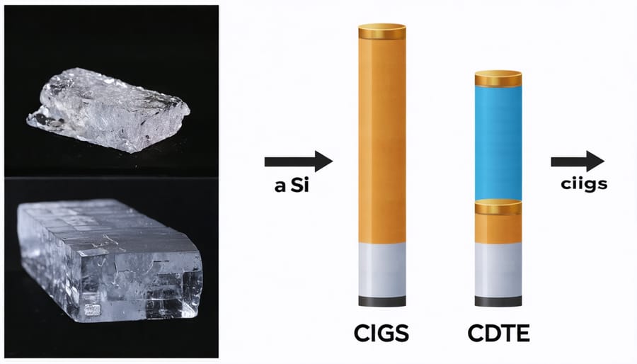
CIGS and CdTe Technologies
CIGS (Copper Indium Gallium Selenide) and CdTe (Cadmium Telluride) technologies represent significant advancements in thin-film solar panel manufacturing. The CIGS production process involves vacuum-based co-evaporation or sputtering deposition of copper, indium, gallium, and selenium onto a glass or flexible substrate. This multi-stage process requires precise temperature control and composition monitoring to achieve optimal efficiency.
CdTe manufacturing typically employs a high-throughput process where cadmium and tellurium compounds are deposited through vapor transport deposition. The process begins with cleaning and preparing a glass substrate, followed by applying a transparent conducting oxide layer. The semiconductor layers are then deposited in a controlled environment at temperatures ranging from 500-600°C.
Both technologies utilize automated production lines with integrated quality control systems. The manufacturing process includes critical steps such as buffer layer deposition, front contact application, and encapsulation. Advanced laser scribing techniques create cell interconnections, while automated visual inspection systems ensure product consistency. These production methods have enabled manufacturers to achieve commercial module efficiencies of 16-18% for CIGS and 14-16% for CdTe, while maintaining cost-effective scalability.
Emerging Materials
The landscape of emerging solar materials continues to evolve rapidly, with perovskites leading the charge in next-generation thin-film technology. These crystalline compounds demonstrate remarkable potential, achieving efficiency rates above 25% in laboratory conditions while offering significantly reduced production costs. Metal halide perovskites, in particular, show promise due to their excellent light absorption properties and simple manufacturing requirements.
Copper Indium Gallium Selenide (CIGS) alternatives are being developed with earth-abundant materials to address supply chain concerns. Research initiatives are exploring bismuth-based compounds and organic semiconductors as sustainable alternatives to traditional materials. These innovations could revolutionize manufacturing processes by enabling solution-processing techniques at lower temperatures, reducing energy consumption during production.
Quantum dot solar cells represent another breakthrough, offering precise bandgap tuning capabilities and the potential for multi-junction devices. Their integration into existing thin-film manufacturing lines could be achieved with minimal modification to current equipment, making them particularly attractive for industrial adoption. These advancements in materials science are driving the industry toward more efficient, cost-effective, and environmentally sustainable production methods.
Quality Control and Testing
In-Line Monitoring
In-line monitoring plays a crucial role in maintaining the quality and efficiency of thin-film solar panel production. Modern manufacturing facilities employ automated quality control systems that continuously monitor critical parameters throughout the deposition process.
Advanced optical inspection systems utilize high-resolution cameras and spectroscopic analysis to detect defects in real-time. These systems can identify microscopic inconsistencies in film thickness, uniformity, and surface quality, allowing for immediate corrective actions during production.
Laser scanning technology measures the electrical properties of the thin films as they are deposited, ensuring optimal conductivity and performance characteristics. Temperature sensors and pressure monitors maintain precise environmental conditions essential for high-quality film formation.
Data analytics software integrates information from multiple monitoring points, creating comprehensive quality profiles for each panel. This enables manufacturers to optimize production parameters and maintain consistent output quality. The system also generates detailed documentation for quality certification and regulatory compliance.
Real-time monitoring significantly reduces waste by identifying issues before they affect large production batches, ultimately improving manufacturing efficiency and reducing costs while ensuring superior product quality.

Post-Production Testing
Post-production testing constitutes a critical phase in thin-film solar panel manufacturing, ensuring each module meets rigorous performance and reliability standards. The process begins with flash testing, where panels are exposed to calibrated light sources that simulate standard test conditions (STC) of 1000 W/m² irradiance at 25°C. This determines the panel’s power output, efficiency, and I-V characteristics.
Electroluminescence imaging follows, utilizing specialized cameras to detect microscopic defects, microcracks, and inactive areas that might compromise long-term performance. Thermal cycling tests subject panels to extreme temperature variations, typically ranging from -40°C to +85°C, to verify their durability and structural integrity.
Quality control engineers conduct humidity freeze testing, exposing panels to high moisture levels and temperature fluctuations to ensure proper encapsulation and weather resistance. Mechanical load testing applies standardized pressure to simulate wind and snow loads, while hail impact testing verifies the module’s resistance to environmental damage.
Final certification testing includes safety compliance verification and performance ratio calculations. Only panels that meet or exceed industry standards receive approval for distribution. Documentation of test results provides crucial data for warranty validation and performance guarantees, establishing confidence in the product’s long-term reliability.
Manufacturing Challenges and Solutions
The manufacturing of thin-film solar panels presents several significant challenges that industry professionals must address to ensure efficient production and high-quality outputs. One of the primary obstacles is maintaining uniform deposition of semiconductor materials across large surface areas. Even minor variations in thickness can lead to reduced efficiency and inconsistent performance across the panel.
Material wastage during the deposition process remains a persistent concern. Traditional vapor deposition methods can result in significant material loss, increasing production costs and environmental impact. To combat this, manufacturers have developed improved techniques such as roll-to-roll processing and advanced spatial atomic layer deposition, which offer better material utilization rates and faster throughput.
Temperature control during manufacturing poses another critical challenge. The precise thermal conditions required for proper film formation must be maintained consistently throughout the production process. Innovative cooling systems and temperature monitoring technologies have been implemented to ensure optimal thermal management, resulting in better crystallization of semiconductor layers and improved overall efficiency.
Contamination control represents a significant manufacturing hurdle. Even microscopic particles can create defects in the thin films, leading to reduced performance or complete panel failure. Advanced clean room technologies and automated handling systems have been developed to minimize contamination risks during production.
The industry has also made substantial progress in addressing encapsulation challenges. Moisture ingress can severely impact the longevity of thin-film panels, particularly in humid environments. New barrier coating technologies and improved edge sealing methods have enhanced the durability of these solar panels significantly.
Quality control automation has emerged as a crucial solution to manufacturing challenges. Advanced imaging systems and artificial intelligence-driven inspection processes can now detect defects in real-time, allowing for immediate corrective actions and reduced waste. These systems have dramatically improved production yields and product consistency.
To address cost concerns, manufacturers have implemented integrated production lines that combine multiple processing steps. This approach reduces handling requirements, minimizes the risk of damage, and increases throughput rates. Additionally, the development of new materials and deposition techniques has helped reduce raw material costs while maintaining or improving panel efficiency.
Looking ahead, collaborative research between industry and academic institutions continues to yield promising solutions for existing manufacturing challenges. Emerging technologies such as quantum dot integration and perovskite-based thin films show potential for revolutionizing production processes while addressing current limitations in efficiency and durability.
The future of thin-film solar manufacturing stands at a promising intersection of technological innovation and market demand. As efficiency rates continue to improve and production costs decrease, manufacturers are investing heavily in advanced automation and Industry 4.0 technologies to streamline operations. The integration of artificial intelligence and machine learning in quality control processes is expected to significantly reduce defect rates while increasing throughput.
Research partnerships between industry leaders and academic institutions are accelerating the development of next-generation materials and deposition techniques. These collaborations are particularly focused on improving the stability and durability of thin-film modules while reducing their environmental impact. The emergence of new semiconducting materials and hybrid architectures suggests potential breakthroughs in conversion efficiency.
Market projections indicate substantial growth in thin-film solar manufacturing capacity over the next decade, particularly in regions with established semiconductor industries. This expansion is driven by increasing demand for building-integrated photovoltaics and flexible solar applications. As manufacturing processes become more refined and standardized, thin-film technology is positioned to play a crucial role in the global transition to renewable energy, offering a compelling combination of versatility, cost-effectiveness, and sustainable production methods.