Discover the remarkable journey of solar energy as we delve into the intricate process of photovoltaic (PV) cell manufacturing. From raw materials to finished modules, this comprehensive overview illuminates the cutting-edge techniques and innovative technologies that transform sunlight into sustainable electricity. Explore the critical stages of silicon purification, wafer fabrication, cell processing, and module assembly, gaining a deep understanding of the scientific principles and engineering marvels behind solar power generation. Join us as we unravel the secrets of PV cell manufacturing, empowering you with the knowledge to navigate the exciting world of renewable energy and contribute to a greener future.
Raw Material Preparation

Silicon Purification
The silicon purification process is crucial in preparing raw silicon for use in solar cells. The most common method is the Siemens process, which involves introducing trichlorosilane gas into a reactor chamber containing high-purity silicon rods heated to around 1,150°C (2,100°F). The gas decomposes and deposits pure silicon onto the rods, which grow into polysilicon ingots with a purity of up to 99.999999%. These ingots are then broken into chunks and melted in a crucible to form monocrystalline or polycrystalline silicon ingots. Another purification method is fluidized bed reactor (FBR) technology, which produces granular polysilicon by decomposing silane gas in a bed of silicon particles. Regardless of the method, the purified silicon serves as the foundation for creating high-efficiency solar cells that convert sunlight into electricity.
Wafer Production
The wafer production process begins with the purified polysilicon, which is melted in a crucible at temperatures exceeding 1,400°C. A seed crystal is dipped into the molten silicon and slowly withdrawn while rotating, forming a cylindrical ingot. The crystalline structure of the resulting ingot depends on the pulling technique used, resulting in either monocrystalline (single crystal) or polycrystalline (multiple crystals) silicon. The ingots are then cut into thin wafers using precision wire saws, with thicknesses typically ranging from 180 to 200 micrometers. The choice between monocrystalline vs polycrystalline wafers impacts the efficiency and cost of the final PV cells. After cutting, the wafers undergo a series of cleaning and etching processes to remove surface damage and contaminants, preparing them for the next steps in the PV cell manufacturing process.

Solar Cell Fabrication
Texturing and Coating
Surface texturing and anti-reflective coatings are critical steps in the PV cell manufacturing process that enhance light absorption and minimize reflection losses. Texturing involves etching the cell surface to create a uniform pattern of microscopic pyramids, which increases the surface area and allows light to bounce between the pyramids, improving the chances of absorption. This is typically achieved through wet chemical etching using solutions like potassium hydroxide or sodium hydroxide. After texturing, an anti-reflective coating, usually composed of silicon nitride or titanium dioxide, is applied to the front surface of the solar cell layers. This thin, transparent coating minimizes reflection by acting as an intermediate layer between the cell and air, effectively reducing the refractive index difference. Together, surface texturing and anti-reflective coatings can increase the cell’s light absorption by up to 20%, significantly improving overall efficiency.
Doping and Electrode Printing
Doping is a crucial step in creating the p-n junction necessary for solar cells to function. This process involves introducing impurities into the silicon wafer to alter its electrical properties. Phosphorus is commonly used for n-type doping, while boron is used for p-type doping. The doping process can be performed through various methods, such as diffusion or ion implantation, to precisely control the dopant concentration and distribution within the silicon wafer.
After doping, the electrical contacts are printed onto the solar cell using a screen printing technique. This process involves applying a conductive paste, typically containing silver, onto the front and back surfaces of the cell through a mesh screen. The front contact is usually designed in a grid pattern to minimize shading while maximizing current collection. The back contact is often a solid layer of aluminum or silver. The printed contacts are then fired at high temperatures to form a strong electrical connection with the silicon wafer. Proper design and printing of the contacts are essential for achieving high efficiency and reliable performance in the finished solar cell.
Cell Testing and Sorting
Once PV cells are manufactured, they undergo rigorous testing to evaluate their performance and efficiency. Specialized equipment measures key parameters such as open-circuit voltage, short-circuit current, fill factor, and power output under standard test conditions. These tests ensure that cells meet the required specifications and perform optimally.
After testing, cells are graded based on their performance characteristics. Grading criteria may include efficiency, current, and voltage outputs. This process allows manufacturers to sort cells into different bins or categories, ensuring consistency and quality control in the final product.
Sorted cells are then carefully packaged and prepared for the next stage of the manufacturing process – module assembly. During this stage, cells with similar characteristics are grouped together to create PV modules with uniform performance. Proper sorting and matching of cells is crucial for optimizing module efficiency and long-term reliability.
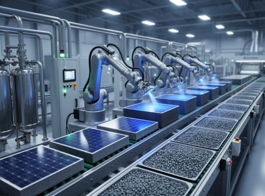
Module Assembly and Encapsulation

Cell Stringing and Tabbing
Cell stringing and tabbing is a crucial step in the PV cell manufacturing process, where individual solar cells are interconnected to form strings. This process involves using thin, flat wires called tabbing ribbons to join the front contact of one cell to the back contact of the adjacent cell. The tabbing ribbons are typically made of tin-coated copper and are soldered onto the cell’s bus bars using automated soldering equipment. The number of cells in a string depends on the desired voltage of the PV module. Once the cells are interconnected, the strings are then connected in parallel to increase the current output. The interconnected strings are then laminated between layers of EVA (ethylene-vinyl acetate) and tempered glass to create a weatherproof and durable PV module. Proper cell stringing and tabbing ensure efficient current flow and minimize resistive losses in the final PV module.
Lamination and Framing
The lamination process is crucial for protecting the delicate solar cells and electrical components from environmental factors. Layers of ethylene-vinyl acetate (EVA) encapsulant are placed above and below the interconnected solar cells, followed by a back sheet and front glass cover. These layers are then heated and pressed together in a laminator, forming a solid, air- and moisture-tight seal around the cells. The laminated module is then fitted into an aluminum frame for additional structural support and ease of installation. The frame also includes a junction box on the back to house the electrical connections. Proper lamination and framing ensure the long-term durability and performance of the solar module, protecting it from physical damage, weather, and corrosion. Quality control checks are performed to verify the integrity of the lamination and framing before the module is ready for final testing and shipment.
Quality Control and Certification
Quality control is an integral part of the PV cell manufacturing process, ensuring that the final product meets the industry’s rigorous performance and safety standards. Manufacturers employ various testing methods to assess the electrical, mechanical, and thermal properties of the PV cells and modules. These tests include current-voltage (I-V) characterization, electroluminescence imaging, and infrared thermography, which help identify defects and performance issues. Additionally, accelerated aging tests simulate real-world conditions to evaluate the long-term durability and reliability of the modules.
PV modules undergo certification processes to comply with international standards such as IEC 61215 for crystalline silicon modules and IEC 61646 for thin-film modules. These certifications cover a wide range of tests, including humidity-freeze, thermal cycling, and mechanical load tests, to ensure the modules can withstand various environmental conditions. Certified modules also undergo safety testing according to standards like IEC 61730 and UL 1703, which assess the modules’ ability to prevent electrical hazards and fire risks.
Stringent quality control measures throughout the manufacturing process, coupled with rigorous performance testing and certification, ensure that PV modules meet the highest industry standards. This commitment to quality assurance instills confidence in consumers and investors, driving the adoption of solar energy as a reliable and sustainable power source.
Conclusion
The PV cell manufacturing process is a complex and precise endeavor that transforms raw materials into high-efficiency solar cells. From the initial production of silicon wafers to the final assembly of solar modules, each step requires strict quality control measures to ensure optimal performance and longevity. Mose Solar’s commitment to educational collaboration with universities and comprehensive training programs helps maintain the highest standards throughout the manufacturing process.
As the demand for clean, renewable energy continues to grow, advancements in PV cell technology will play a crucial role in shaping the future of the solar industry. Ongoing research and development efforts aim to improve cell efficiency, reduce manufacturing costs, and develop new materials that can further enhance the performance of solar modules. By staying at the forefront of these innovations, manufacturers like Mose Solar can continue to deliver cutting-edge PV solutions that meet the evolving needs of the market while contributing to a more sustainable future.