Discover the remarkable science behind photovoltaic (PV) cells, the building blocks of solar energy. In this comprehensive article, we delve into the intricate process of PV cell construction, from raw materials to cutting-edge manufacturing techniques. Uncover the secrets of how silicon, the second most abundant element on Earth, is transformed into highly efficient solar cells capable of harnessing the sun’s energy. Explore the critical components that make up a PV cell, including the semiconductor layers, electrical contacts, and protective coatings. Step inside state-of-the-art fabrication facilities where precision engineering and stringent quality control measures ensure the production of high-performance solar cells. Join us on this fascinating journey as we unveil the groundbreaking advancements in PV cell construction that are revolutionizing the renewable energy landscape and paving the way for a cleaner, greener future.
Key Components of a PV Cell

Substrate
The substrate is the foundation layer upon which the photovoltaic cell is built. It provides mechanical support and serves as a base for depositing the active layers of the cell. The most commonly used substrate material for PV cells is silicon, which can be either monocrystalline or polycrystalline. Monocrystalline silicon substrates are made from a single crystal of silicon, resulting in higher efficiency but also higher production costs. Polycrystalline silicon substrates, on the other hand, are composed of multiple silicon crystals and offer a more cost-effective option, albeit with slightly lower efficiency. The choice of substrate material depends on the desired performance, cost, and application of the PV cell.
Semiconductor Layers
The heart of a PV cell lies in its semiconductor layers, typically made of silicon. When sunlight strikes these layers, the photons energize the electrons within the silicon atoms, causing them to break free from their orbits. The cell’s unique structure, consisting of two distinct semiconductor layers – one positively charged (p-type) and one negatively charged (n-type) – creates an electric field at their junction. This field drives the freed electrons to flow in a specific direction, generating an electric current. The semiconductor layers are carefully engineered to optimize photon absorption and electron flow, maximizing the cell’s efficiency in converting solar energy into usable electricity. Advances in materials science and manufacturing techniques continue to improve the performance and cost-effectiveness of these crucial components, pushing the boundaries of solar cell technology and making solar power an increasingly attractive alternative to traditional energy sources.
Electrical Contacts
Electrical contacts are essential components in PV cell construction, responsible for capturing and transferring the generated current from the cell to the external circuit. These contacts are typically made of highly conductive materials, such as silver, aluminum, or copper, and are strategically placed on the front and back surfaces of the cell. The front contact is usually a grid-like pattern of thin metal fingers that allows light to pass through while minimizing shading, while the back contact is a solid layer covering the entire rear surface. Proper design and application of electrical contacts are crucial for maximizing cell efficiency and minimizing resistive losses. Advanced techniques, such as screen printing or photolithography, are employed to precisely deposit the contacts onto the cell surfaces, ensuring optimal current collection and transfer. The quality and durability of electrical contacts play a significant role in the overall performance and longevity of PV cells and modules.
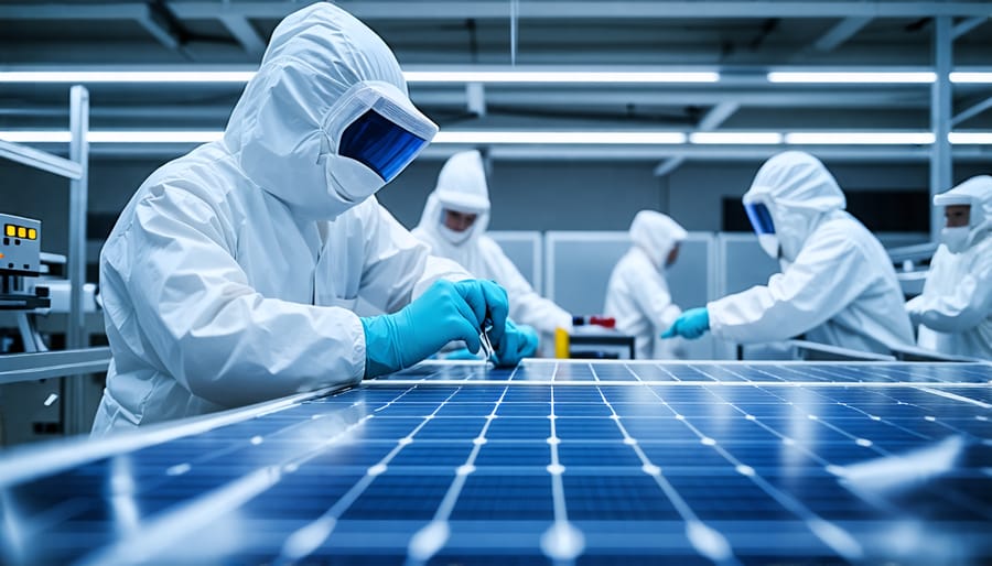
PV Cell Manufacturing Process
Wafer Production
The wafer production process begins with high-purity silicon, typically derived from quartz sand. The silicon is melted and formed into ingots using one of two methods: Czochralski growth for monocrystalline wafers or directional solidification for polycrystalline wafers. In the Czochralski process, a seed crystal is dipped into the molten silicon and slowly pulled upward, allowing a cylindrical ingot to form. For polycrystalline wafers, the molten silicon is cast into a square mold and allowed to cool gradually. The resulting ingots are then cut into thin wafers using precision wire saws. These wafers undergo a series of cleaning, etching, and polishing steps to remove impurities and create a uniform surface. The wafers are then doped with small amounts of boron or phosphorus to create the necessary p-type and n-type semiconductors. This doping process is essential for establishing the electrical properties that enable the photovoltaic effect. The doped wafers serve as the foundation for the subsequent cell fabrication steps, where additional layers and contacts are added to create a functional solar cell.
Doping and Layer Deposition
Doping and layer deposition are crucial steps in PV cell construction that introduce impurities and apply additional semiconductor layers to enhance the cell’s performance. The doping process involves introducing controlled amounts of impurities, such as boron or phosphorus, into the semiconductor material to create p-type and n-type regions. These regions form the p-n junction, which is essential for the cell’s ability to generate an electric current when exposed to sunlight.
After doping, additional layers of semiconductor materials are deposited onto the cell using techniques such as chemical vapor deposition (CVD) or physical vapor deposition (PVD). These layers, which may include intrinsic (undoped) and heavily doped regions, help to optimize the cell’s efficiency by improving charge carrier collection and minimizing recombination losses.
The precise control of doping concentrations and the quality of the deposited layers are critical factors in determining the overall performance of the PV cell. Advanced techniques, such as ion implantation and atomic layer deposition (ALD), are increasingly being used to achieve higher precision and uniformity in these processes. By carefully engineering the doping profiles and layer structures, researchers and manufacturers can continue to push the boundaries of PV cell efficiency and cost-effectiveness.
Contact Application
After the front and back surface have been properly prepared, the electrical contacts are applied to allow the generated current to be collected and channeled out of the cell. The front contact consists of a fine metal grid, typically made of silver, that is screen printed onto the cell surface. This grid must be carefully designed to minimize shading while providing sufficient electrical conductivity. The back contact is usually a full-surface aluminum layer that is also screen printed and then sintered at high temperatures to form a good electrical connection with the silicon. These contacts are critical for efficient current extraction and play a major role in the overall performance of the PV cell.
To further enhance the electrical properties of the contacts, additional thin layers may be deposited between the silicon and the metal contacts. These interface layers, such as titanium dioxide or silicon dioxide, help to reduce recombination losses and improve contact adhesion. Once the front and back contacts are in place, the PV cell is essentially complete and ready for testing and integration into a module. The quality and consistency of the electrical contacts are closely monitored throughout the manufacturing process to ensure high cell efficiency and reliability in the final product.
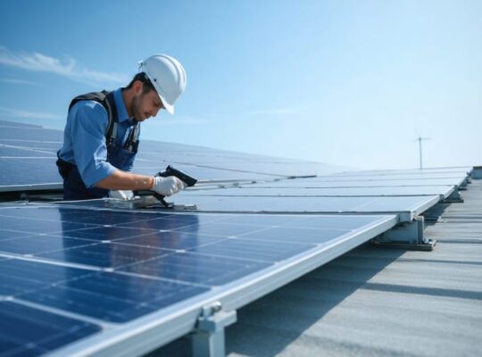
From Cells to Modules
From the individual photovoltaic cells, the next step in PV module construction is connecting and packaging these cells into functional solar panels. This process involves several key steps to ensure optimal power output, durability, and longevity of the finished product.
First, the PV cells are electrically connected in series using thin, flat wires or metal ribbons. These interconnections are carefully soldered to the front and back contacts of each cell, allowing electrons to flow from one cell to the next. The number of cells connected in series determines the voltage of the module, while the number of parallel cell strings determines the current.
Once connected, the cell matrix is laminated between sheets of ethylene-vinyl acetate (EVA) and tempered glass on the front, with a polymer backsheet on the rear. This encapsulation protects the cells from environmental factors like moisture, dust, and mechanical stress. The lamination process involves applying heat and pressure to melt the EVA, bonding the layers together.
The laminated cell matrix is then framed, typically using anodized aluminum, to provide structural support and easy installation. Junction boxes are attached to the back of the module, housing the output terminals and bypass diodes that protect the cells from overheating due to shading or damage.
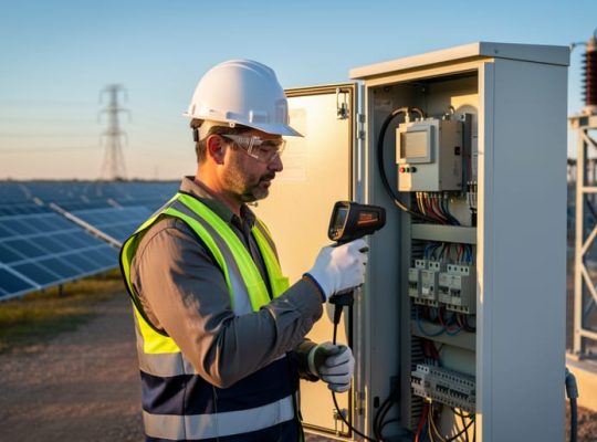
Finally, the completed PV module undergoes rigorous quality testing to ensure it meets performance and safety standards before being shipped for installation. By connecting and packaging individual cells into larger modules, PV manufacturers create a durable, efficient product that can withstand the elements and generate clean electricity for decades.

Conclusion
The field of photovoltaics is rapidly advancing, with new innovations in PV cell technology constantly pushing the boundaries of efficiency and cost-effectiveness. As researchers and manufacturers continue to refine materials, optimize manufacturing processes, and develop novel cell architectures, the future of solar energy looks brighter than ever. With ongoing advancements in areas such as perovskite cells, tandem cells, and bifacial modules, the potential for more affordable, high-performance PV systems is immense. As the world increasingly turns to renewable energy solutions to combat climate change and meet growing energy demands, the role of photovoltaic technology in shaping a sustainable future cannot be overstated.