The photovoltaic manufacturing industry stands at a critical juncture where environmental responsibility directly intersects with economic viability. Zero waste production represents a paradigm shift that transforms conventional solar panel manufacturing from a linear resource-consumption model into a circular ecosystem where every material input serves a purpose and nothing exits as waste. This approach transcends simple recycling initiatives—it fundamentally redesigns production processes to eliminate waste generation at the source, recover valuable materials from production byproducts, and establish closed-loop systems that continuously reuse resources.
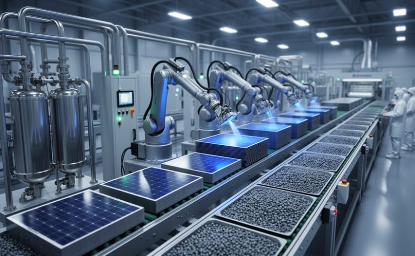
Manufacturing solar panels ironically generates significant waste through silicon sawdust, chemical slurries, broken wafers, and edge trims. Traditional facilities can lose up to 40% of polysilicon during wafer production alone. Zero waste methodologies address this paradox by implementing advanced recovery systems, optimizing cutting technologies, and developing new applications for manufacturing residuals. These sustainable manufacturing practices not only reduce environmental impact but also substantially lower production costs through improved material utilization and resource efficiency.
The transition requires systematic integration of waste prevention strategies across every production stage, from raw material processing through module assembly. Success demands technological innovation, workforce training, and collaborative partnerships between manufacturers, research institutions, and equipment suppliers. As global demand for photovoltaic systems accelerates, implementing zero waste production becomes essential for manufacturers seeking competitive advantage while fulfilling their role in building a genuinely sustainable energy future.
Understanding Zero Waste Production in Solar Manufacturing
What Qualifies as Waste in PV Production
Understanding waste streams in photovoltaic manufacturing is essential for developing effective zero waste strategies. The solar panel manufacturing process generates distinct waste categories at each production stage, with varying environmental and economic impacts.
Silicon kerf loss represents one of the most significant waste streams, occurring during wafer slicing. Traditional wire sawing methods generate approximately 40-50% material loss as silicon powder mixed with cutting fluids. In modern facilities, this translates to roughly 6-8 grams of silicon waste per wafer produced. Diamond wire sawing technology has reduced this percentage to 30-35%, though the volume remains substantial given production scales.
Broken wafers and cracked cells constitute another major category, typically accounting for 3-8% of total production volume. These mechanical failures occur during handling, transportation between processing stations, and thermal stress from high-temperature treatments. Manufacturing lines producing 10,000 wafers daily may experience 300-800 units requiring rejection or downgrading.
Chemical byproducts from texturing, etching, and cleaning processes generate both liquid and gaseous waste streams. Hydrofluoric acid mixtures, alkaline solutions, and solvents require careful handling and disposal. Industry studies indicate that producing one square meter of solar cells consumes 1,500-3,000 liters of ultrapure water and generates corresponding wastewater volumes.
Packaging materials, including protective films, cardboard separators, and shipping containers, add 2-4% to total waste by weight. End-of-line module rejects from electrical testing, visual inspection, or lamination defects typically represent 1-3% of finished production. Collectively, these waste streams can account for material losses exceeding 50% from raw silicon to final module output, highlighting substantial improvement opportunities.
The Business Case Beyond Environmental Benefits
While zero waste production delivers significant reductions to the environmental impact of photovoltaic manufacturing, the economic advantages often provide the most compelling justification for implementation. Forward-thinking manufacturers recognize that sustainable practices directly enhance profitability through multiple channels.
Raw material cost savings represent the most immediate financial benefit. Silicon reclamation systems can recover up to 95% of kerf loss during wafer slicing, potentially saving manufacturers $3-5 million annually per gigawatt of production capacity. Companies like REC Silicon have documented material cost reductions exceeding 30% through comprehensive waste recovery programs.
Disposal costs decrease substantially when waste streams are eliminated. Traditional landfill fees and hazardous waste management expenses can account for 2-4% of production costs. Zero waste initiatives redirect these expenses toward recovery infrastructure that generates long-term value.
New revenue streams emerge from selling recovered materials. Purified silicon, reclaimed metals, and processed chemicals command market prices that offset recovery system investments. Leading manufacturers report recovery system payback periods of 18-36 months.
Brand reputation advantages cannot be understated in today’s market. Sustainability certifications and verified zero waste achievements differentiate manufacturers in competitive bidding processes, particularly for large-scale projects with environmental procurement requirements. Industry data indicates that certified zero waste facilities experience 15-20% higher customer retention rates and preferential treatment from environmentally conscious buyers, creating sustainable competitive advantages that extend well beyond immediate cost savings.
Silicon Waste Reduction and Recovery Strategies
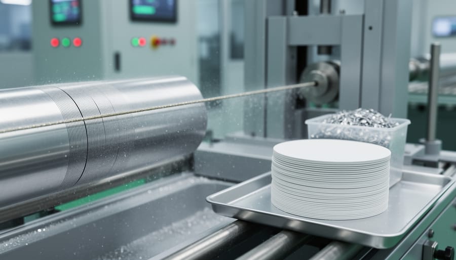
Diamond Wire Sawing Technology
Diamond wire sawing represents one of the most significant technological advances in reducing material waste during silicon wafer production. Traditional slurry-based sawing methods generate kerf loss—the material lost during cutting—of 200 micrometers or more per cut. In contrast, diamond wire sawing technology reduces this loss to under 100 micrometers, effectively doubling the number of wafers that can be produced from a single silicon ingot.
This technology employs steel wires embedded with industrial diamonds to slice through silicon with remarkable precision. The thinner cutting width not only conserves valuable silicon material but also reduces the environmental impact associated with mining and processing additional raw materials. For manufacturers, this translates to substantial cost savings and improved sustainability metrics.
Industry adoption has accelerated significantly in recent years, with diamond wire sawing now accounting for over 90 percent of monocrystalline wafer production globally. The technology has proven particularly effective for monocrystalline silicon, though polycrystalline applications have also benefited from advancements in wire composition and cutting parameters.
Technical considerations include initial capital investment in specialized equipment, wire quality and replacement schedules, and optimization of cutting speeds to balance productivity with surface quality. Operators must also manage heat dissipation during cutting and ensure proper wire tension throughout the process. Despite these challenges, the material savings and enhanced throughput make diamond wire sawing an essential component of zero waste manufacturing strategies in photovoltaic production.
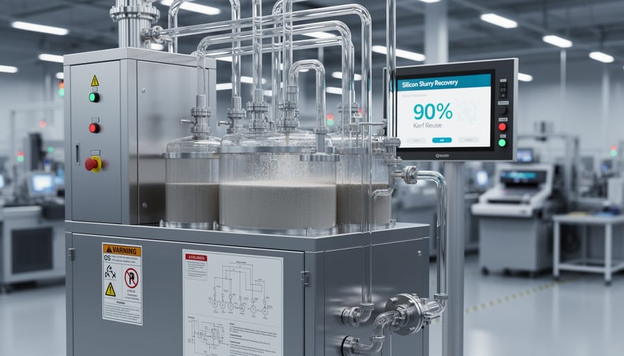
Silicon Slurry Recovery and Purification
Silicon wafer slicing generates significant quantities of cutting slurry—a mixture containing silicon carbide abrasives, polyethylene glycol coolant, and valuable silicon particles. Recovering this silicon represents both an environmental imperative and economic opportunity, as cutting waste can contain 40-50% of the original silicon ingot material.
The recovery process begins with mechanical filtration to separate larger silicon particles from the liquid carrier. Advanced centrifugation systems then extract finer particles, achieving separation efficiencies exceeding 95%. The recovered silicon undergoes chemical treatment to remove organic contaminants and abrasive materials. This typically involves acid washing with hydrochloric or sulfuric acid solutions, followed by alkaline treatment to eliminate remaining impurities.
Recrystallization transforms the recovered silicon into usable feedstock. Through controlled thermal processing, the purified silicon particles are melted and reformed into polysilicon or reintegrated into new ingots. Modern purification techniques can restore silicon purity levels to 99.9999% (6N), meeting stringent photovoltaic-grade requirements. Some facilities collaborate with universities to develop innovative purification methods that reduce energy consumption while maintaining quality standards.
Current industry reintegration rates vary considerably, ranging from 60% to 85% depending on facility capabilities and quality control protocols. Leading manufacturers have achieved closed-loop systems where virtually all recovered silicon returns to production. However, achieving consistent quality remains challenging, as trace contaminants can affect cell efficiency.
The economic viability of silicon recovery has improved substantially as purification technologies mature and virgin silicon prices fluctuate. Processing costs have decreased by approximately 30% over the past five years, making recovery economically competitive with purchasing new feedstock. This progress demonstrates that environmental stewardship and profitability can align when supported by proper technological infrastructure and commitment to sustainable manufacturing practices.
Cell and Module Production Waste Minimization
Defect Prevention Through Process Control
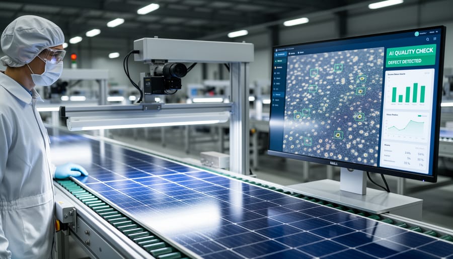
Defect prevention represents a cornerstone of zero waste production in photovoltaic manufacturing, where advanced monitoring systems work continuously to identify and eliminate quality issues before they result in scrap. Modern facilities employ real-time Statistical Process Control (SPC) that monitors critical parameters across every production stage, from wafer thickness to cell efficiency metrics. These systems establish control limits based on historical data and immediately flag deviations, allowing operators to make adjustments before defects propagate through the production line.
AI-powered quality inspection systems have revolutionized defect detection, using machine learning algorithms trained on millions of images to identify microcracks, contamination, and surface irregularities invisible to human inspectors. These systems achieve detection accuracies exceeding 99.5%, catching defects that would otherwise become waste at later stages when material value has increased significantly.
Predictive maintenance programs complement quality control by preventing equipment-related defects. By analyzing vibration patterns, thermal signatures, and performance trends, facilities can schedule maintenance before equipment degradation affects product quality. Leading manufacturers implementing comprehensive process control report defect rate reductions from industry averages of 3-5% down to below 1%, translating to substantial waste prevention and cost savings. Universities collaborating with industry partners contribute valuable research on advanced sensing technologies and optimization algorithms that continue improving these prevention capabilities.
Repurposing Rejected Components
When photovoltaic cells or modules fail to meet premium grade specifications, manufacturers have developed sophisticated strategies to maximize their value rather than discarding them entirely. Grade-B cells, which may have minor cosmetic imperfections or slightly reduced efficiency ratings, find new purpose in applications where absolute peak performance is less critical. These components frequently serve residential installations, off-grid systems, or educational demonstrations where cost considerations outweigh marginal efficiency differences.
Module-level defects often prove repairable through targeted intervention. Encapsulation bubbles, minor frame damage, or junction box issues can be corrected through specialized repair protocols, allowing these units to enter secondary markets with appropriate warranties. This practice extends product lifecycles while generating revenue streams that would otherwise be lost.
For irreparable components, material harvesting represents the final recovery opportunity. Advanced disassembly techniques allow manufacturers to extract valuable materials including silicon wafers, aluminum frames, copper wiring, and glass panels. Silicon recovered from rejected cells can be reprocessed into lower-grade applications or new ingots, while metals return to commodity markets. Even damaged glass finds applications in aggregate materials or fiberglass production.
Secondary markets for downgraded components continue expanding globally. Developing regions benefit from access to affordable solar technology, while budget-conscious consumers in established markets find value in certified refurbished products. Collaboration with universities creates additional outlets, as educational institutions utilize grade-B components for hands-on training programs without compromising learning outcomes. These partnerships simultaneously address waste reduction goals while advancing workforce development in photovoltaic technology.
Chemical and Water Management Systems
Closed-Loop Water Recycling
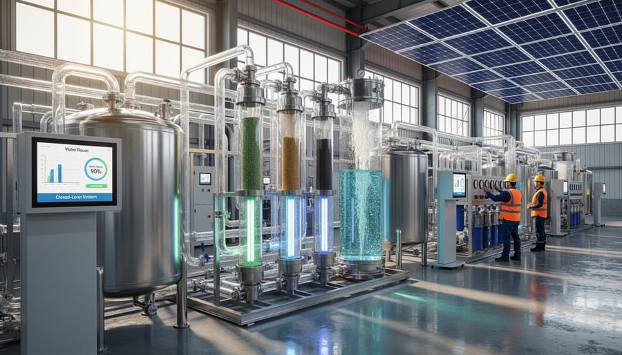
Water represents one of the most critical resources in photovoltaic manufacturing, with silicon wafer processing alone consuming thousands of liters per production cycle. Advanced closed-loop water recycling systems now enable manufacturers to achieve reuse rates exceeding 90%, dramatically reducing both freshwater consumption and wastewater discharge.
Modern water treatment systems employ a multi-barrier approach combining several proven technologies. Reverse osmosis serves as the primary purification method, using semi-permeable membranes to remove up to 99% of dissolved solids, ionic contaminants, and particles. This technology proves particularly effective for reclaiming water from rinsing operations in wafer cleaning and texturing processes. Deionization regeneration complements reverse osmosis by removing remaining ionic impurities through ion exchange resins, which can be continuously regenerated using acid and base solutions rather than replaced, minimizing chemical waste.
Multi-stage filtration systems incorporate progressively finer filters, starting with sediment removal at 50 microns, followed by activated carbon filtration for organic compounds, and concluding with ultrafiltration at 0.01 microns. This staged approach extends membrane life and optimizes treatment efficiency across varying contamination levels.
Implementation costs typically range from $500,000 to $2 million for mid-scale facilities, depending on water volume requirements and existing infrastructure. However, payback periods average 2-4 years when factoring in reduced freshwater purchasing costs, lower wastewater treatment fees, and decreased regulatory compliance expenses. Many manufacturers working with university research partners have demonstrated that combining these technologies with real-time water quality monitoring systems can push reuse rates beyond 95%, approaching true zero-liquid-discharge operations while maintaining the ultrapure water standards essential for high-efficiency solar cell production.
Chemical Recovery and Neutralization
Chemical recovery systems play a vital role in minimizing hazardous waste while supporting sustainable clean production methods in photovoltaic manufacturing. Modern facilities employ advanced techniques to reclaim and reuse chemicals from key production processes, particularly those involving texturing, cleaning, and etching operations.
Acid recovery systems utilize distillation, membrane separation, and ion exchange technologies to reclaim hydrofluoric and nitric acids used in wafer texturing. These processes can achieve recovery rates exceeding 90%, substantially reducing both raw material costs and hazardous waste generation. Similarly, alkaline solutions containing potassium hydroxide or sodium hydroxide undergo regeneration through evaporation and reconcentration, extending their operational lifespan.
Solvent recovery presents another significant opportunity, with isopropyl alcohol and other cleaning agents recovered through distillation units integrated directly into production lines. These closed-loop systems maintain chemical purity while eliminating continuous discharge.
For chemicals that cannot be economically recovered, neutralization protocols ensure safe disposal. Acid-base neutralization reactions convert hazardous materials into stable salts suitable for standard wastewater treatment. Precipitation methods remove heavy metals and other contaminants before discharge.
Compliance with environmental regulations requires comprehensive monitoring systems, including real-time pH sensors, chemical concentration analyzers, and automated control systems. Regular audits and documentation verify adherence to local, national, and international environmental standards such as ISO 14001. Partnerships with certified waste management contractors ensure proper handling of residual materials requiring off-site treatment, maintaining environmental responsibility throughout the disposal chain.
Packaging and Logistics Waste Reduction
Reusable Packaging Solutions
The photovoltaic industry is transitioning from single-use cardboard boxes and foam inserts toward durable, multi-trip packaging systems that significantly reduce material waste. These reusable solutions typically consist of rigid plastic containers, aluminum frames, and custom-fitted dividers engineered to withstand 50-100+ shipping cycles. Leading manufacturers report that while initial investment in reusable packaging ranges from 3-5 times higher than disposable alternatives, the cost amortizes over multiple uses, achieving break-even within 18-24 months and delivering substantial savings thereafter.
Implementing reusable packaging requires establishing reverse logistics networks to retrieve, inspect, clean, and redistribute containers. This infrastructure challenge necessitates strategic partnerships with logistics providers and coordination across supply chain stakeholders. Advanced tracking systems using RFID tags or QR codes monitor container location, usage cycles, and maintenance needs, ensuring optimal fleet management.
Universities collaborating with industry leaders have developed lifecycle assessments demonstrating that reusable packaging systems reduce material consumption by 85-95% compared to single-use alternatives while cutting transportation emissions through optimized container design. The transition demands upfront capital investment and operational restructuring, but delivers measurable environmental benefits alongside long-term economic advantages. Educational programs now incorporate reverse logistics principles, preparing professionals to design and manage these circular packaging systems effectively within photovoltaic manufacturing operations.
Implementing a Zero Waste Program: Practical Steps
Waste Auditing and Baseline Establishment
Implementing a robust waste auditing system forms the foundation of any successful zero waste production strategy in photovoltaic manufacturing. The process begins with a comprehensive facility assessment, documenting all waste generation points across the production line—from silicon wafer processing to module assembly and packaging operations.
The first step involves assembling a cross-functional audit team including production managers, environmental specialists, and quality control personnel. This team systematically maps waste streams over a minimum 30-day period to capture production variability and seasonal fluctuations. Each waste stream requires categorization by type (silicon kerf, broken cells, chemical effluents, packaging materials), volume, and contamination level, establishing a detailed material flow analysis.
Quantitative measurement proves essential for establishing meaningful baselines. Recommended metrics include total waste generated per megawatt of production capacity, recycling rate percentage, landfill diversion rate, and waste-to-revenue ratio for recovered materials. Digital tracking systems, integrated with existing manufacturing execution systems, enable real-time monitoring and trend analysis.
Research institutions and universities collaborating with industry leaders have developed standardized waste classification frameworks specifically for PV manufacturing. These frameworks ensure consistency when benchmarking against industry standards and regulatory requirements.
Based on audit findings, facilities should establish SMART reduction targets—specific, measurable, achievable, relevant, and time-bound objectives. Industry best practices suggest initial targets of 25-40% waste reduction within the first year, with progressive goals toward 90% landfill diversion rates. Regular quarterly reviews enable teams to adjust strategies, identify emerging waste streams, and maintain momentum toward comprehensive zero waste objectives.
Cross-Functional Team Development
Successful zero waste implementation in photovoltaic manufacturing requires deliberate organizational restructuring that breaks down traditional departmental silos. Establishing cross-functional teams that integrate production engineers, quality control specialists, environmental managers, and operations staff creates the collaborative framework necessary for identifying waste streams and developing comprehensive solutions. These teams should include representatives from procurement, maintenance, and design engineering to address waste prevention at every stage of the production cycle.
Clear role definition proves essential for accountability and progress tracking. Designate waste reduction champions within each production area who monitor metrics, coordinate with the central sustainability team, and facilitate continuous improvement initiatives. Plant managers must allocate dedicated time and resources for team members to engage in waste analysis activities without compromising production schedules.
Change management strategies should prioritize transparent communication about environmental goals and their connection to operational efficiency and cost savings. Regular training programs must equip workers with practical skills in waste segregation, equipment optimization, and problem identification. Many organizations partner with universities to develop customized training modules that address specific manufacturing challenges while building broader environmental literacy among the workforce.
Employee engagement mechanisms, including suggestion programs and recognition systems, transform workers from passive participants into active innovators. When frontline staff understand their direct impact on waste reduction outcomes, they contribute valuable insights that management-level planning often overlooks, creating a culture of continuous environmental improvement.
Certification Standards and Third-Party Verification
Third-party verification through established certification programs provides credible validation of zero waste achievements in photovoltaic manufacturing. The TRUE (Total Resource Use and Efficiency) certification, administered by Green Business Certification Inc., represents the most comprehensive zero waste standard globally. This program offers platinum (100% diversion), gold (90-99%), silver (75-89%), and certified (50-74%) levels based on waste diversion rates. Similarly, UL 2799 provides standardized verification for organizations claiming zero waste to landfill, zero waste, or waste reduction achievements.
The certification process requires detailed documentation of waste streams, diversion methods, and disposal practices. Independent auditors conduct on-site inspections, reviewing material flow data, vendor contracts for recycling and recovery services, and waste tracking systems. Facilities must demonstrate continuous improvement plans and maintain transparent reporting protocols.
Achieving certified status delivers substantial competitive advantages for PV manufacturers. Certification enhances corporate reputation, satisfies increasingly stringent supply chain requirements from major solar developers, and demonstrates environmental leadership to stakeholders. Universities collaborating on sustainability research often prioritize partnerships with certified facilities, creating opportunities for innovation development. Educational programs frequently showcase certified operations as case studies, further elevating industry recognition and attracting environmentally conscious talent to the renewable energy sector.
Educational Pathways for Zero Waste Manufacturing Professionals
Pursuing a career in zero waste photovoltaic manufacturing requires specialized knowledge spanning materials science, process engineering, and environmental management. Educational institutions increasingly recognize this demand, developing comprehensive curricula that prepare professionals for sustainability-focused roles in the solar industry.
Academic programs in renewable energy engineering, sustainable manufacturing, or materials science provide foundational knowledge essential for zero waste production roles. Coursework typically includes modules on circular economy principles, lifecycle assessment methodologies, resource efficiency optimization, and waste stream characterization. Advanced programs offer specialized training in photovoltaic-specific topics such as silicon reclamation, chemical recovery systems, and closed-loop manufacturing processes.
Professional certifications enhance career prospects in this field. The Certified Energy Manager (CEM) and LEED Green Associate credentials demonstrate commitment to sustainable practices, while Six Sigma and Lean Manufacturing certifications provide methodologies applicable to waste reduction initiatives. Industry-specific programs focusing on photovoltaic technology and sustainable production practices offer targeted skill development.
Collaborative programs between manufacturers and educational institutions create valuable experiential learning opportunities. Many solar companies partner with universities to offer internships, cooperative education placements, and research projects centered on waste minimization technologies. These partnerships enable students to apply theoretical knowledge in operational settings while contributing to real-world sustainability improvements.
Continuing education remains crucial as zero waste technologies evolve. Professionals benefit from workshops, webinars, and industry conferences that address emerging innovations in waste valorization, advanced recycling techniques, and sustainable supply chain management. This ongoing learning ensures practitioners maintain expertise in the rapidly advancing field of zero waste photovoltaic manufacturing.
Zero waste production represents a fundamental transformation in how the photovoltaic industry approaches manufacturing, moving beyond traditional linear models toward truly circular systems. The evidence presented throughout this exploration demonstrates that zero waste is not merely an environmental aspiration but a practical, economically viable strategy that enhances operational efficiency while reducing ecological impact. Companies implementing comprehensive waste reduction programs consistently report decreased material costs, improved resource utilization, and strengthened market positioning as sustainability becomes increasingly central to procurement decisions.
The convergence of advanced technologies—from silicon recycling systems and closed-loop water treatment to AI-driven process optimization—has made near-zero waste operations achievable across the entire PV manufacturing value chain. As industry leaders demonstrate success with these approaches, we anticipate accelerated adoption throughout 2024 and beyond, driven by both regulatory requirements and competitive advantages. Emerging innovations in perovskite recycling, chemical recovery systems, and integrated manufacturing platforms promise to further minimize waste generation while maintaining production quality.
For aspiring professionals and current practitioners alike, engaging with zero waste principles offers significant career opportunities in this rapidly evolving field. Educational programs focused on sustainable manufacturing methodologies, often developed through university collaborations, provide essential knowledge for implementing these systems effectively. Whether you are a researcher investigating novel recycling technologies, an engineer optimizing production processes, or a sustainability manager developing implementation strategies, your contribution to advancing zero waste practices directly shapes the renewable energy transition. The path toward sustainable PV manufacturing requires collective commitment, continuous learning, and willingness to embrace innovative solutions that benefit both industry performance and environmental stewardship.