Solar energy manufacturing stands at an inflection point where production innovations directly determine the technology’s accessibility, affordability, and global adoption potential. The photovoltaic industry has achieved remarkable cost reductions—dropping from $76 per watt in 1977 to under $0.30 per watt today—through systematic manufacturing improvements that span material science breakthroughs, automated production processes, and advanced facility designs.
Manufacturing efficiency drives this transformation. When production lines increase throughput by 15-20% through robotic automation, those savings cascade to consumers as lower system prices. When perovskite-silicon tandem cells achieve 33% efficiency in laboratory settings and approach commercial viability, manufacturers must redesign entire production workflows to accommodate new deposition techniques and quality control protocols.
The current landscape encompasses three interconnected domains: materials innovation introducing alternative semiconductors and sustainable raw material sourcing, process optimization deploying artificial intelligence for defect detection and yield improvement, and smart manufacturing facilities that reduce energy consumption during production itself. These advances respond to urgent market demands—renewable energy must scale from 29% of global electricity generation to over 60% by 2030 to meet climate targets.
This transformation requires more than technological capability. It demands skilled professionals who understand both the science of photovoltaic cells and the economics of mass production. Universities and industry leaders now collaborate to develop comprehensive training programs that prepare the workforce for this manufacturing evolution, ensuring innovations transition smoothly from research laboratories to gigawatt-scale production facilities serving millions of consumers worldwide.
The Economics Behind Solar Manufacturing Efficiency
Breaking Down the Cost Structure
Understanding the cost structure of solar panel manufacturing reveals where efficiency improvements deliver maximum value. Material costs traditionally represent 40-45% of the total panel price, with silicon wafers accounting for roughly 25-30% alone. Manufacturing labor and overhead comprise approximately 20-25%, while research and development, quality control, and administrative expenses make up the remaining 30-35%.
Recent innovations in cell efficiency directly impact this equation. When manufacturers increase conversion efficiency from 20% to 23%, the cost per watt decreases significantly because the same material inputs generate more power output. This efficiency dividend cascades through the entire cost structure—reducing installation expenses per watt, lowering balance-of-system costs, and improving return on investment for end users.
The most substantial impact emerges from automation investments that simultaneously reduce labor costs and improve consistency. Advanced manufacturing facilities report 15-20% cost reductions through automated quality control systems and precision deposition techniques. These improvements particularly benefit materials utilization, where reducing silicon waste by even 2-3% translates to millions in annual savings for high-volume manufacturers. Academic partnerships increasingly focus on optimizing these manufacturing parameters, helping translate laboratory innovations into commercially viable production improvements.
The Manufacturing-to-Market Pipeline
Manufacturing efficiency improvements in solar panel production create a cascading effect that ultimately benefits end consumers through reduced pricing and enhanced market accessibility. As production costs decrease through automation, advanced materials, and streamlined processes, manufacturers can offer more competitive pricing while maintaining healthy profit margins. Recent industry data demonstrates that production efficiency gains of 20-30% can translate to consumer price reductions of 15-25%, making solar installations increasingly affordable for residential and commercial applications.
This manufacturing-to-market pipeline operates on economies of scale, where higher production volumes enabled by efficient processes further drive down per-unit costs. The competitive pressure within the photovoltaic industry compels manufacturers to pass these savings along to consumers, accelerating market adoption. Additionally, improved manufacturing quality control reduces warranty claims and system failures, lowering long-term ownership costs for consumers. As production facilities implement innovative technologies and workforce training programs, the entire supply chain becomes more responsive to market demands, ensuring that technological breakthroughs reach customers faster and at more accessible price points.
Revolutionary Materials Processing Techniques
Advanced Silicon Wafer Production
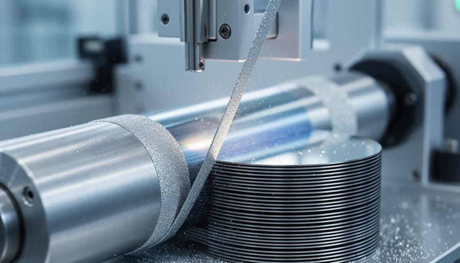
Silicon wafer production has undergone revolutionary transformations that directly impact solar panel efficiency and cost-effectiveness. The industry has moved decisively toward diamond wire sawing technology, replacing traditional slurry-based cutting methods. This innovation utilizes ultra-thin diamond-coated wires that slice through silicon ingots with remarkable precision, reducing material waste by up to 50% compared to conventional techniques.
Modern manufacturing facilities now produce wafers measuring just 120-160 micrometers in thickness, down from the 200+ micrometer standard of previous generations. These thinner wafers maintain structural integrity while maximizing the number of cells produced from each silicon ingot. The reduction represents a significant economic advantage, as raw silicon constitutes a substantial portion of production costs.
Kerf loss—the material transformed into unusable dust during cutting—has decreased dramatically through advanced sawing parameters and wire tension optimization. Contemporary processes achieve kerf widths below 100 micrometers, preserving valuable silicon that would otherwise become waste. This efficiency translates directly into lower manufacturing costs and reduced environmental impact.
Leading manufacturers have invested heavily in automated handling systems that protect these increasingly delicate wafers throughout production. Computer-controlled processes monitor thickness uniformity and detect micro-cracks before they compromise cell performance. These quality control measures ensure that material savings do not compromise product reliability.
Universities collaborating with industry leaders have developed computational models that optimize cutting speeds and wire characteristics, pushing the boundaries of what’s technically achievable while maintaining commercial viability. These partnerships between academic research and manufacturing expertise continue driving innovations that benefit the entire photovoltaic sector.
PERC Cell Manufacturing Optimization
Modern PERC cell technology manufacturing has undergone significant optimization through automation and precision engineering. Advanced screen printing techniques now enable more uniform application of passivation layers, reducing material waste by up to 20% while improving cell efficiency consistency across production batches. Laser ablation systems have replaced traditional mechanical processes, creating cleaner contact openings with minimal damage to the underlying silicon structure.
Inline quality monitoring systems equipped with artificial intelligence algorithms detect surface defects in real-time, allowing immediate adjustments to manufacturing parameters before entire batches are compromised. These systems analyze thousands of data points per second, identifying microcracks, incomplete passivation, or contamination that human inspectors might miss.
Throughput improvements stem from parallel processing lines and optimized thermal treatment cycles that reduce production time per cell by 30%. Universities collaborating with manufacturers have developed predictive maintenance protocols that minimize equipment downtime, while industry training programs ensure operators understand both the technical fundamentals and practical troubleshooting techniques essential for maintaining high-yield production environments in this competitive market.
Automated Quality Control Systems
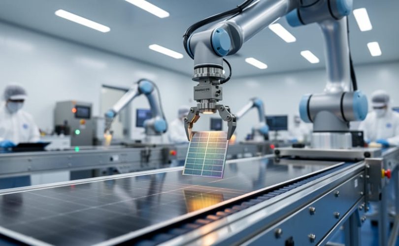
Modern photovoltaic manufacturing increasingly relies on AI-powered inspection systems that transform quality assurance from reactive to proactive. These automated platforms utilize machine vision and deep learning algorithms to scan every solar cell and module at multiple production stages, detecting microscopic defects invisible to human inspectors. Real-time monitoring capabilities identify issues like microcracks, busbar misalignments, and soldering inconsistencies within milliseconds, enabling immediate corrective action before defective units progress through the production line. This early intervention dramatically reduces material waste and rework costs while maintaining consistent output quality. Leading manufacturers report defect detection rates exceeding 99.5 percent, compared to 85-90 percent with manual inspection methods. The systems continuously learn from production data, refining detection parameters and predicting potential equipment failures before they impact manufacturing. Universities partnering with solar manufacturers integrate these quality control technologies into research programs, preparing the next generation of photovoltaic professionals to leverage automated systems effectively. This convergence of artificial intelligence and manufacturing excellence represents a fundamental shift toward zero-defect production standards in the solar industry.
Energy-Efficient Manufacturing Facilities
Clean Room Energy Optimization
Photovoltaic manufacturing facilities require stringent environmental controls to maintain the ultra-clean conditions necessary for producing high-efficiency solar cells. These clean rooms traditionally consume enormous amounts of energy through continuous air filtration, temperature regulation, and humidity control. However, recent innovations are substantially reducing this energy burden while maintaining the ISO Class 5 or better conditions essential for semiconductor-grade manufacturing.
Advanced HVAC systems now incorporate variable frequency drives and intelligent sensor networks that adjust airflow based on real-time particulate monitoring rather than operating at maximum capacity continuously. This demand-responsive approach can reduce ventilation energy consumption by 30-40% compared to conventional systems. Modern clean room designs also feature modular air handling units that allow zone-specific control, eliminating the need to condition entire facilities uniformly when only specific production areas require strict environmental parameters.
LED lighting retrofits have become standard in newer facilities, delivering energy savings exceeding 60% while producing minimal heat that would otherwise require additional cooling capacity. Some manufacturers have implemented daylight harvesting systems that integrate natural light with automated dimming controls, further reducing electrical demand during daytime production shifts.
Thermal recovery systems represent another significant advancement, capturing waste heat from manufacturing equipment and repurposing it for space heating or pre-conditioning incoming air. Combined with improved insulation materials and air curtain technologies that minimize contamination risks at entry points, these integrated solutions demonstrate how manufacturing efficiency innovations directly support the industry’s sustainability mission while reducing production costs.
Closed-Loop Water and Chemical Systems
Modern photovoltaic manufacturing facilities are implementing closed-loop systems that dramatically reduce water consumption and chemical waste while lowering production costs. These innovative recycling and recovery technologies capture, purify, and reuse resources that were traditionally discharged as waste, transforming solar panel manufacturing into a more sustainable operation.
Water recycling systems now achieve recovery rates exceeding 90 percent in advanced facilities. Through multi-stage filtration and purification processes, manufacturing water used for cell cleaning and wafer cutting returns to production-grade quality. This approach reduces freshwater intake by millions of gallons annually per facility, proving particularly valuable in water-stressed regions where solar manufacturing is expanding.
Chemical recovery systems similarly reclaim valuable materials from processing solutions. Silicon tetrachloride, a byproduct of polysilicon production, undergoes conversion back into usable feedstock rather than requiring costly disposal. Etching solutions and cleaning agents pass through regeneration units that remove contaminants while preserving active compounds, extending chemical lifecycles by 300 to 500 percent.
Leading manufacturers partner with universities to advance closed-loop technologies through research initiatives that optimize recovery efficiency and develop new purification methods. These collaborations inform educational programs training the next generation of engineers in sustainable manufacturing practices. The economic benefits are substantial, with facilities reporting 20 to 40 percent reductions in raw material costs alongside significant environmental improvements, demonstrating that resource conservation and profitability align effectively in modern solar production.
Next-Generation Module Assembly Innovations
Precision Cell Interconnection Methods
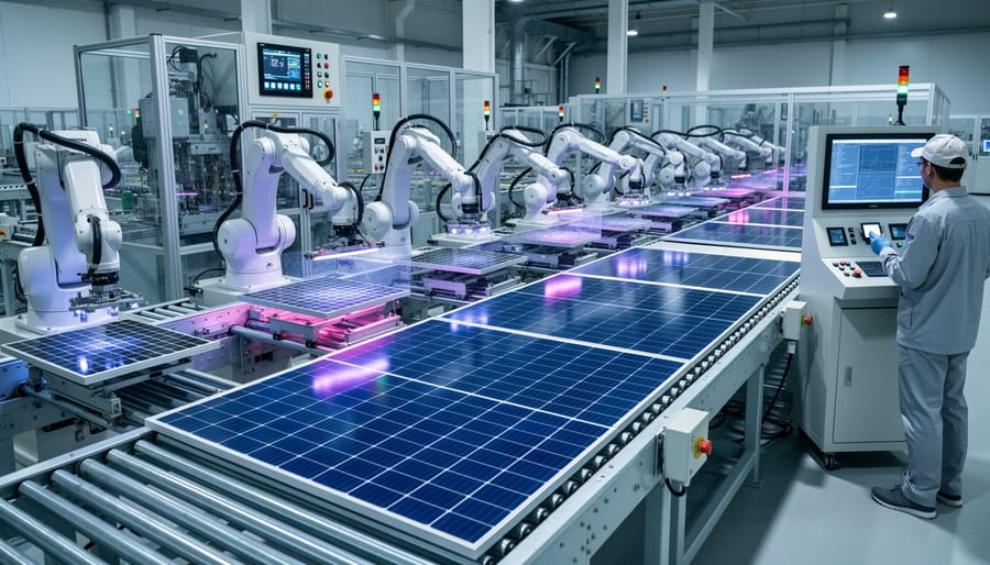
Modern cell interconnection techniques represent a significant advancement in photovoltaic manufacturing, reducing material waste while enhancing module durability. Traditional soldering methods are being replaced by multi-busbar and smart wire connection technologies that utilize narrower ribbons and eliminate up to 30% of silver consumption per module. These innovations decrease electrical resistance and minimize mechanical stress on delicate silicon cells during thermal cycling.
Leading manufacturers now employ automated stringing equipment integrated with digital twin technology to optimize connection parameters in real-time. Electrically conductive adhesives are emerging as alternatives to conventional soldering, operating at lower temperatures and reducing thermal damage risks. Shingled cell designs, where cells are overlapped and bonded with adhesive films, eliminate visible busbars entirely while improving module efficiency by increasing active surface area.
Through smart factory implementation, manufacturers achieve precision placement tolerances within micrometers, ensuring consistent electrical performance across production runs. Universities collaborating with industry partners are developing next-generation interconnection methods using laser welding and ultrasonic bonding, further advancing manufacturing reliability and sustainability objectives.
Advanced Encapsulation Technologies
Modern encapsulation technologies represent a critical advancement in solar panel longevity and sustainability. Traditional ethylene-vinyl acetate encapsulants are being replaced with innovative thermoplastic polyolefin and polyolefin elastomer materials that offer superior moisture resistance and enhanced ultraviolet stability. These next-generation encapsulants extend panel operational life from 25 to 35 years while maintaining optical transparency and electrical insulation properties.
Manufacturing processes have evolved significantly through the adoption of vacuum lamination techniques and automated quality control systems that detect microscopic defects before they compromise panel integrity. Cross-linking polymer technology creates molecular bonds that withstand thermal cycling and mechanical stress more effectively than conventional materials.
The environmental benefits extend beyond performance improvements. Advanced encapsulation processes reduce energy consumption during production by up to 30 percent compared to traditional methods, while enabling easier end-of-life recycling. Research collaborations between manufacturers and academic institutions continue to refine formulations that balance cost-effectiveness with enhanced protective capabilities. These developments directly support manufacturers in producing more durable products while reducing their carbon footprint, demonstrating how material science innovations drive both economic and environmental progress in the photovoltaic industry.
Building-Integrated PV Manufacturing
Building-integrated photovoltaics represent a paradigm shift in solar manufacturing, requiring specialized production techniques that merge architectural aesthetics with photovoltaic performance. Unlike conventional panels, solar tiles and roof shingles must satisfy dual requirements: generating electricity efficiently while maintaining visual appeal and structural integrity as building materials.
Manufacturing these products involves laminating thin-film or crystalline silicon cells onto durable substrates that mimic traditional roofing materials. Advanced coating processes ensure weather resistance and UV stability while preserving cell efficiency. Leading manufacturers have developed proprietary techniques to integrate junction boxes and wiring systems within the tiles themselves, eliminating visible connectors that compromise architectural design.
The production challenge centers on achieving consistent electrical performance across smaller, irregularly shaped modules while maintaining cost competitiveness with standard panels. Universities collaborate with manufacturers to optimize cell cutting patterns that minimize silicon waste and develop adhesives that withstand thermal cycling without degrading electrical connections.
Quality control protocols for building-integrated products extend beyond electrical testing to include impact resistance, fire ratings, and water infiltration assessments. This comprehensive approach ensures products meet both electrical codes and building standards, expanding solar adoption among homeowners who prioritize curb appeal alongside sustainability.
Digital Transformation in PV Production
Smart Factory Implementation
Modern solar manufacturing facilities are revolutionizing production efficiency through integrated smart factory technologies that combine IoT sensors, machine learning algorithms, and automated systems. These advanced facilities continuously monitor production parameters such as temperature, humidity, material flow, and equipment performance, enabling manufacturers to identify bottlenecks and optimize operations in real-time.
Machine learning algorithms analyze vast datasets from production lines to predict maintenance needs, reduce defects, and improve yield rates. For instance, AI-powered quality control systems can detect microscopic imperfections in solar cells that human inspectors might miss, ensuring only premium products reach the market. These systems learn from historical data to anticipate potential issues before they impact production, significantly reducing downtime and material waste.
Integration between different manufacturing stages creates seamless workflows where equipment communicates autonomously to adjust processes based on demand fluctuations and material availability. Universities collaborating with industry leaders are developing specialized training programs that prepare photovoltaic professionals to operate and maintain these sophisticated systems. Educational initiatives focus on data analytics, automation engineering, and IoT infrastructure management, ensuring the workforce evolves alongside technological advancement. This convergence of digital innovation and solar manufacturing expertise positions the industry for unprecedented scalability and cost efficiency while maintaining rigorous quality standards.
Supply Chain Optimization
Advanced digital platforms are revolutionizing supply chain management in solar manufacturing by integrating real-time data analytics, predictive modeling, and blockchain technology. These systems enable manufacturers to track raw materials from extraction through final product delivery, reducing inventory carrying costs by up to 30% while minimizing waste throughout the production cycle.
Machine learning algorithms now forecast demand patterns with unprecedented accuracy, allowing manufacturers to optimize procurement schedules and reduce material obsolescence. Smart inventory management systems automatically adjust ordering parameters based on production schedules, seasonal variations, and market trends, ensuring just-in-time delivery without compromising manufacturing continuity.
Transportation optimization software analyzes multiple variables including route efficiency, carbon footprint, and delivery schedules to minimize environmental impact while reducing logistics costs. Some manufacturers have achieved 25% reductions in transportation-related emissions through algorithmic route planning and consolidated shipping strategies.
Collaborative platforms connect manufacturers directly with raw material suppliers, eliminating intermediary delays and improving transparency. These systems provide complete material traceability, supporting ethical sourcing initiatives and enabling rapid response to supply disruptions. Universities partnering with industry leaders are developing specialized courses in sustainable supply chain management, preparing professionals to implement these sophisticated systems effectively. This integration of digital tools with workforce education ensures continuous improvement in supply chain efficiency across the solar manufacturing sector.
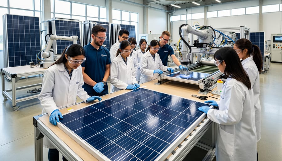
Training the Next Generation of Manufacturing Professionals
Skills Gap in Advanced Manufacturing
Modern photovoltaic manufacturing facilities require specialized technical competencies that extend far beyond traditional manufacturing skills. The industry faces a pronounced shortage of professionals trained in semiconductor processing, thin-film deposition techniques, and automated quality control systems specific to solar cell production. Critical gaps exist in understanding advanced materials characterization, where technicians must interpret data from spectroscopic analysis and quantum efficiency testing to optimize production parameters.
Process engineers need expertise in cleanroom protocols, vacuum technology, and precision coating methods including PECVD and screen printing techniques. Additionally, the shift toward smart manufacturing demands proficiency in data analytics, machine learning applications for predictive maintenance, and integration of Industry 4.0 technologies. Addressing these competency gaps requires collaboration with universities to develop curriculum that bridges theoretical knowledge with hands-on experience in PV-specific equipment and processes. Technical training programs must emphasize both fundamental semiconductor physics and practical troubleshooting skills, while educational program offerings should include certifications in solar manufacturing standards, quality assurance methodologies, and emerging technologies like perovskite processing and heterojunction cell fabrication.
University-Industry Educational Partnerships
Strategic partnerships between universities and solar manufacturers are reshaping workforce development in the photovoltaic sector. Leading institutions now offer specialized curricula combining materials science, automation engineering, and clean energy principles to prepare graduates for advanced manufacturing roles. These collaborative programs provide students with hands-on experience using industry-standard equipment, from automated cell testing systems to precision deposition technologies.
Manufacturing efficiency innovations require professionals who understand both theoretical foundations and practical implementation. Industry-sponsored research projects allow students to tackle real-world challenges, such as optimizing production line throughput or reducing material waste in cell fabrication. Many programs include internships at solar manufacturing facilities, where participants gain direct exposure to lean manufacturing principles and quality control protocols.
Corporate partnerships also facilitate knowledge transfer in reverse, as academic researchers share breakthrough findings in perovskite stability, bifacial module optimization, and advanced metallization techniques. Joint training initiatives ensure existing workforce members stay current with emerging technologies, while certification programs validate competencies in specialized areas like automated optical inspection and predictive maintenance systems. This ecosystem approach accelerates the adoption of manufacturing innovations while building a talent pipeline capable of driving continuous improvement across the solar industry.
The convergence of manufacturing innovations across materials science, production automation, facility design, and workforce development creates a multiplier effect that extends far beyond individual improvements. When advanced silicon purification techniques combine with automated assembly lines and smart factory systems, the resulting efficiency gains compound exponentially rather than additively. This synergistic relationship demonstrates how each breakthrough strengthens the foundation for subsequent advances, establishing a virtuous cycle of innovation that continuously drives the industry forward.
The trajectory of future improvements points toward unprecedented levels of production efficiency and cost reduction. Manufacturing facilities now achieve throughput rates that seemed impossible a decade ago, while maintaining higher quality standards and lower defect rates. These operational improvements directly translate into more affordable solar installations for consumers and businesses, fundamentally expanding accessibility to clean energy solutions. As production costs decrease by even marginal percentages, millions of additional households worldwide gain economic access to photovoltaic technology.
The interconnection between production efficiency, cost reduction, and market accessibility forms the cornerstone of solar energy’s expanding global reach. Universities collaborating with manufacturers play a crucial role in this ecosystem, developing both technological innovations and the skilled workforce needed to implement them. Educational programs focused on advanced manufacturing techniques ensure that knowledge transfer keeps pace with technological advancement, creating sustainable pathways for continued industry growth. This holistic approach—where manufacturing excellence, economic viability, and human capital development work in concert—positions solar energy as an increasingly dominant force in the global transition toward sustainable power generation.