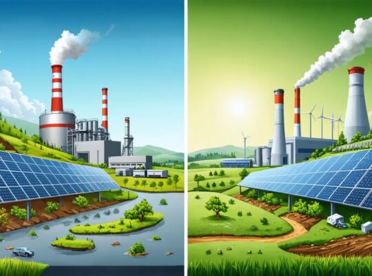
The performance gap between monocrystalline and amorphous solar panels originates in their fundamentally different manufacturing processes, where silicon crystal structure determines everything from efficiency ratings to real-world applications. Monocrystalline technology produces panels reaching 20-22% efficiency through precision cultivation of single silicon crystals, while amorphous thin-film variants achieve 6-10% efficiency by depositing non-crystalline silicon layers onto substrates.
Understanding this manufacturing distinction matters because production methods directly influence cost structures, energy payback periods, material requirements, and optimal deployment scenarios. Monocrystalline panels require energy-intensive Czochralski or float-zone processes that grow uniform silicon ingots, creating superior electron mobility and power density. Amorphous panels utilize chemical vapor deposition or sputtering techniques that consume significantly less silicon and enable flexible, lightweight form factors unsuitable for crystalline alternatives.
This comparison extends beyond laboratory specifications into practical considerations for system designers, project developers, and procurement specialists. The crystalline structure debate encompasses thermal coefficients, degradation patterns, low-light performance characteristics, and total lifecycle economics. While monocrystalline panels dominate residential and commercial installations where space constraints prioritize efficiency, amorphous technology serves specialized applications requiring conformability, partial shade tolerance, or reduced weight loads.
The following analysis examines how manufacturing processes create these performance divergences, equipping professionals with technical knowledge to specify appropriate technologies for distinct project requirements and environmental conditions.
Understanding Solar Cell Technology: The Crystalline Advantage
What Makes Monocrystalline Panels Different
Monocrystalline panels derive their distinctive performance characteristics from their fundamental material structure: a single, continuous crystal lattice of silicon. Unlike other photovoltaic technologies, these panels are manufactured from cylindrical silicon ingots grown through the Czochralski process, where a seed crystal is slowly pulled from molten silicon to create a uniform crystalline structure.
This single-crystal arrangement allows electrons to move through the material with minimal resistance and scattering. The uniform atomic alignment creates clear pathways for electron flow, resulting in conversion efficiencies typically ranging from 17% to 22% in commercial applications, with laboratory versions exceeding 26%. The lack of grain boundaries, which are present in monocrystalline vs polycrystalline comparisons as a key differentiator, means fewer opportunities for electron recombination and energy loss.
The high-purity silicon required for monocrystalline production, typically 99.9999% pure, further enhances electrical performance. This purity level, combined with the ordered crystal structure, enables superior performance in low-light conditions and better temperature coefficients. However, these advantages come at increased production costs, as the manufacturing process requires precise temperature control and longer production times than alternative technologies.
The Amorphous Silicon Alternative
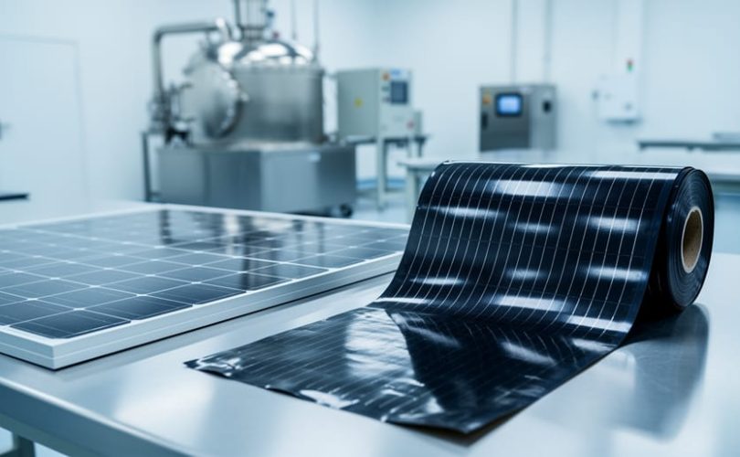
Amorphous silicon technology represents a fundamentally different approach to photovoltaic manufacturing. Unlike crystalline panels that rely on structured silicon atoms arranged in uniform lattice patterns, amorphous silicon consists of silicon atoms in a disordered, non-crystalline state. This distinctive structure emerges during production when silicon is deposited as an extremely thin film onto substrates like glass, metal, or plastic through chemical vapor deposition processes.
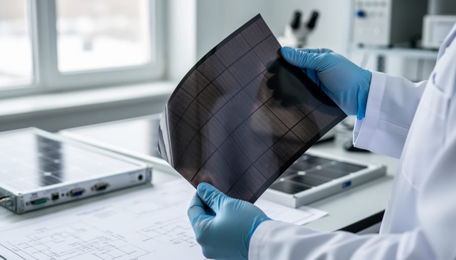
The absence of a crystalline structure significantly influences the material’s photovoltaic properties. Amorphous silicon absorbs light more efficiently across certain wavelengths due to its disordered atomic arrangement, allowing manufacturers to create much thinner active layers—typically just one micrometer compared to the 200-micrometer wafers used in monocrystalline panels. This thin-film characteristic reduces material costs substantially and enables flexible manufacturing applications.
However, the non-crystalline structure also introduces inherent limitations. The random arrangement of silicon atoms creates more defect sites and dangling bonds within the material, which trap charge carriers and reduce overall conversion efficiency to approximately 6-9% in commercial applications. Research institutions collaborating with universities continue investigating hydrogenation techniques and multi-junction configurations to mitigate these structural disadvantages while maintaining the technology’s manufacturing advantages.
Monocrystalline Panel Production: From Silicon to High-Efficiency Modules
The Czochralski Process: Growing Single Crystal Ingots
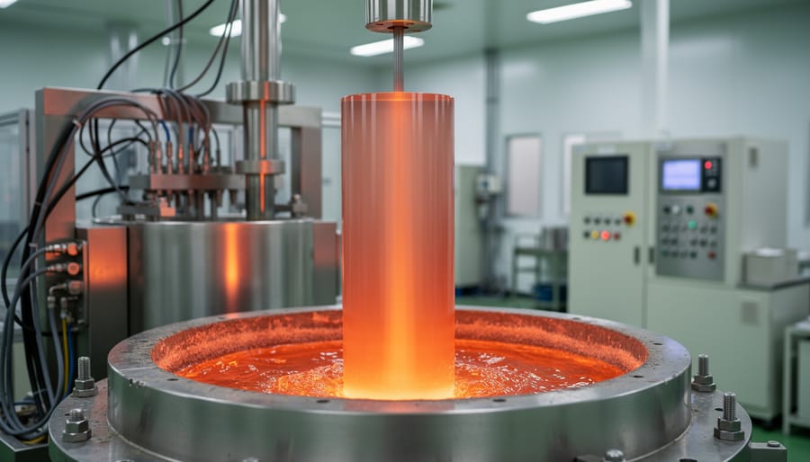
The Czochralski process represents the cornerstone of monocrystalline silicon production, enabling the creation of highly uniform crystal structures essential for efficient solar cells. Named after Polish scientist Jan Czochralski, this method involves melting ultra-pure polysilicon in a quartz crucible at temperatures exceeding 1,400 degrees Celsius.
The process begins by dipping a small seed crystal of silicon into the molten material. As the seed crystal slowly rotates and withdraws from the melt at precisely controlled rates—typically one to two millimeters per minute—silicon atoms from the liquid align themselves with the seed’s crystal lattice structure. This atomic alignment propagates throughout the growing ingot, creating a single, continuous crystal structure.
Temperature control proves critical throughout this operation. The furnace maintains thermal gradients within fractions of a degree to prevent crystal defects or polycrystalline formation. Industrial Czochralski furnaces can grow cylindrical ingots measuring 200 to 300 millimeters in diameter and up to two meters in length, with the entire growth process taking 24 to 48 hours.
The resulting ingot exhibits uniform crystallographic orientation throughout its entire volume, meaning every silicon atom occupies a predictable position relative to its neighbors. This structural uniformity directly translates to superior electrical properties, as electrons can move through the material with minimal interference from grain boundaries or structural irregularities. This fundamental difference in atomic organization distinguishes monocrystalline silicon from its amorphous counterpart, where silicon atoms arrange randomly without long-range order, significantly impacting the performance characteristics of the final solar panels.
Wafer Slicing and Cell Fabrication
Following ingot formation, the crystalline silicon undergoes precision wafer slicing, a critical stage in solar cell manufacturing that distinguishes monocrystalline from amorphous technologies. For monocrystalline cells, diamond wire saws cut the cylindrical ingots into ultra-thin wafers, typically 160-200 micrometers thick. This sawing process inevitably generates material loss, or kerf, representing one cost factor in monocrystalline production. Amorphous silicon, conversely, bypasses this step entirely through direct deposition onto substrates.
Once sliced, monocrystalline wafers undergo doping, where controlled amounts of phosphorus and boron are diffused into the silicon to create the p-n junction essential for photovoltaic conversion. This process typically occurs in high-temperature diffusion furnaces at temperatures exceeding 800 degrees Celsius, establishing the electric field that separates photo-generated electron-hole pairs.
The final enhancement involves applying an anti-reflective coating, usually silicon nitride, through plasma-enhanced chemical vapor deposition. This coating serves dual purposes: reducing surface reflection from approximately 35% to below 3%, thereby maximizing light absorption, and providing surface passivation to minimize carrier recombination. The characteristic blue tint of monocrystalline panels results from this coating’s optical properties.
These precision manufacturing steps contribute to monocrystalline cells achieving efficiencies of 20-22% in commercial applications, substantially higher than amorphous silicon’s 6-9% efficiency range, while simultaneously explaining the cost differential between these technologies.
Module Assembly and Quality Control
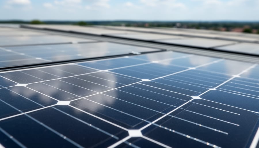
The final assembly stage fundamentally differs between monocrystalline and amorphous technologies, reflecting their distinct structural characteristics. For monocrystalline modules, manufacturers employ automated soldering systems to interconnect individual cells using conductive ribbons, typically copper coated with tin-silver alloys. These ribbons create series connections that build voltage across the panel while maintaining electrical continuity. The interconnected cell matrix is then encapsulated between protective layers: ethylene vinyl acetate (EVA) sheeting bonds the cells to low-iron tempered glass on the front surface and a weather-resistant backsheet, creating a hermetic seal that prevents moisture ingress and mechanical damage.
Amorphous thin-film modules follow a different approach. Since deposition occurs directly onto large substrates, cell interconnection happens during the manufacturing process through laser scribing that creates monolithic integration. The substrate itself becomes part of the finished module, requiring only edge sealing and junction box attachment.
Quality control protocols include electroluminescence imaging to detect microcracks, flash testing to verify electrical parameters against nameplate ratings, and accelerated aging tests simulating decades of environmental exposure. These procedures ensure modules meet IEC 61215 standards for crystalline silicon and IEC 61646 for thin-film technologies, guaranteeing performance warranties that extend 25 years for monocrystalline and typically 10-15 years for amorphous products.
Advanced Manufacturing: PERC and Bifacial Technologies
Modern monocrystalline manufacturing has undergone significant advancement through the integration of PERC technology, which represents a substantial leap beyond traditional cell architectures. This innovation adds a passivation layer to the rear surface of the solar cell, reducing electron recombination and improving light capture through enhanced rear-side reflection. Manufacturing facilities implementing PERC processes achieve efficiency gains of 1-2 percentage points compared to standard cells, pushing commercial monocrystalline panels beyond 22% efficiency.
The PERC manufacturing process integrates seamlessly into existing production lines with additional deposition and laser processing steps. This compatibility has accelerated industry-wide adoption, making PERC the dominant monocrystalline technology in current production. Furthermore, bifacial cell designs building upon PERC architecture enable electricity generation from both panel surfaces, capturing reflected light from surrounding environments. These bifacial modules can increase energy yield by 10-30% depending on installation conditions and albedo factors, representing the cutting edge of monocrystalline development. Such technological refinements starkly contrast with amorphous silicon, where fundamental material limitations prevent comparable efficiency advancement regardless of manufacturing innovations applied.
Amorphous Panel Production: The Thin-Film Approach
Vapor Deposition: Creating Non-Crystalline Layers
Amorphous silicon production relies on vapor deposition techniques that fundamentally differ from the energy-intensive crystal growing processes used in monocrystalline manufacturing. This method allows manufacturers to create non-crystalline photovoltaic layers at significantly lower temperatures, typically between 200-400°C compared to the 1400°C required for crystalline silicon.
Chemical vapor deposition (CVD) represents the most common approach in thin-film manufacturing. During this process, silane gas (SiH4) is introduced into a vacuum chamber containing the substrate material, which can be glass, metal, or flexible polymer. When the silane gas decomposes under controlled conditions, silicon atoms deposit randomly onto the substrate surface, forming a thin amorphous layer without organized crystal structure.
Plasma-enhanced chemical vapor deposition (PECVD) further refines this technique by using radio frequency energy to create plasma that accelerates the deposition process. This enhancement enables better control over layer thickness and hydrogen content, which directly influences the material’s electronic properties. The plasma energizes the reactive gases, allowing deposition at even lower temperatures while maintaining film quality.
Physical vapor deposition (PVD) offers an alternative method where silicon is physically vaporized through sputtering or evaporation, then condensed onto the substrate. Research institutions collaborating with industry partners continue developing advanced deposition techniques that improve efficiency and reduce production costs, making amorphous silicon increasingly viable for large-scale applications.
Production Advantages and Limitations
The manufacturing distinctions between monocrystalline and amorphous silicon technologies create significant trade-offs in production efficiency, material requirements, and final product characteristics.
Amorphous silicon production offers compelling manufacturing advantages. The process operates at substantially lower temperatures—typically between 200-300°C compared to the 1400°C+ required for monocrystalline crystal growth. This reduced thermal demand translates to lower energy consumption during fabrication and enables deposition onto temperature-sensitive substrates like plastics and flexible materials. The thin-film deposition technique used for amorphous silicon requires approximately 1% of the silicon material needed for crystalline technologies, addressing both cost and resource efficiency concerns. Furthermore, large-area deposition methods allow for continuous roll-to-roll manufacturing, reducing production time and enabling novel applications on curved or flexible surfaces.
However, these production advantages come with performance compromises. The disordered atomic structure inherent to amorphous silicon results in lower carrier mobility and higher recombination rates, directly limiting conversion efficiency to 6-10% compared to monocrystalline’s 20-22%. Additionally, amorphous modules experience the Staebler-Wronski effect—a photodegradation phenomenon causing 10-30% efficiency loss during initial sun exposure before stabilization.
Monocrystalline production, while energy-intensive and material-demanding, creates the precise crystalline lattice structure necessary for superior electron flow and sustained high performance. This fundamental relationship between manufacturing process and semiconductor quality explains why monocrystalline technology dominates applications where space efficiency and long-term power output justify higher production costs, while amorphous silicon serves specialized niches requiring flexibility or low-light performance.
Performance Comparison: How Manufacturing Determines Real-World Results
Efficiency and Power Output
The performance gap between monocrystalline and amorphous solar panels stems directly from their fundamental manufacturing differences. Monocrystalline panels consistently achieve conversion efficiency rates of 18-22%, while amorphous thin-film technology typically delivers 6-10% efficiency. This substantial disparity originates at the atomic level.
Monocrystalline silicon’s superior efficiency results from its highly ordered crystal structure, created through the energy-intensive Czochralski process. This uniform lattice allows electrons to move freely with minimal resistance, maximizing photon-to-electron conversion. The pure, defect-free crystalline arrangement enables optimal light absorption and charge carrier mobility, directly translating to higher power output per square meter.
Conversely, amorphous silicon lacks this ordered structure. During plasma-enhanced chemical vapor deposition, silicon atoms arrange randomly without defined crystal patterns. This disordered atomic arrangement creates numerous dangling bonds and defect states that trap electrons, significantly reducing charge carrier mobility and overall conversion efficiency. However, the manufacturing simplicity and reduced material requirements make amorphous technology economically viable for specific applications where space constraints are minimal.
Understanding these manufacturing-level distinctions helps professionals and researchers identify appropriate applications for each technology, balancing efficiency requirements against production costs and installation parameters.

Degradation Rates and Longevity
Crystal structure profoundly influences panel longevity, with monocrystalline modules demonstrating superior long-term stability. Industry data reveals monocrystalline panels typically degrade at 0.3-0.5% annually, maintaining approximately 85-90% of original capacity after 25 years. This minimal degradation stems from their ordered atomic structure, which resists defect formation and performance loss over extended operational periods.
Amorphous silicon faces significantly higher degradation challenges, primarily due to the Staebler-Wronski effect. This phenomenon occurs when light exposure creates metastable defects in the disordered silicon network, reducing conversion efficiency by 10-30% during initial operation. While manufacturers pre-stabilize modules to minimize this impact, amorphous panels still experience higher overall degradation rates of 0.5-1.0% annually. Research conducted through university collaborations has demonstrated that temperature cycling and moisture ingress accelerate degradation in amorphous structures more rapidly than crystalline alternatives.
The manufacturing differences directly explain these longevity disparities. Monocrystalline production creates fewer inherent defects, establishing a more robust foundation for sustained performance. Amorphous deposition, while enabling flexible applications and lower production costs, inherently produces less stable atomic arrangements. For photovoltaic professionals evaluating lifecycle economics, understanding these degradation mechanisms proves essential for accurate system design and return-on-investment calculations across different deployment scenarios.
Temperature Performance and Environmental Resilience
The manufacturing processes for monocrystalline and amorphous solar panels create fundamentally different material structures that significantly impact their temperature performance and environmental resilience. These differences stem directly from the crystalline arrangements established during production.
Monocrystalline panels typically exhibit temperature coefficients ranging from -0.3% to -0.5% per degree Celsius above 25°C. This performance characteristic results from the uniform crystal lattice structure created during the Czochralski process. The ordered silicon arrangement facilitates consistent electron movement, but this same precision makes the material more sensitive to thermal agitation. As temperatures rise, the increased atomic vibration in the crystalline structure impedes charge carrier mobility, causing predictable efficiency losses.
In contrast, amorphous silicon demonstrates superior temperature coefficients, typically between -0.2% to -0.25% per degree Celsius. The disordered atomic structure produced during vapor deposition paradoxically provides an advantage in high-temperature environments. The random silicon arrangement already experiences minimal long-range electron transport, making the material less susceptible to thermal disruption.
Environmental resilience follows similar patterns rooted in manufacturing origins. The rigid crystalline structure of monocrystalline cells offers excellent durability and resistance to physical degradation over 25-30 years. However, amorphous panels, despite their flexible substrate compatibility, experience more pronounced degradation within the first year, a phenomenon called the Staebler-Wronski effect. This initial efficiency loss of 10-30% occurs as light exposure creates metastable defects in the disordered silicon network, eventually stabilizing at reduced but consistent performance levels.
Cost Analysis: Manufacturing Economics and ROI
Production Costs and Market Pricing
Manufacturing costs differ substantially between these technologies, directly influencing market accessibility. Monocrystalline panels require energy-intensive production processes, including the Czochralski method for growing single-crystal silicon ingots and precision wafer slicing. These sophisticated procedures result in higher manufacturing expenses, typically translating to premium consumer pricing ranging from $1.00 to $1.50 per watt.
In contrast, amorphous silicon production involves depositing thin layers of silicon onto substrates through plasma-enhanced chemical vapor deposition, a significantly less energy-intensive process. This streamlined manufacturing reduces production costs by approximately 40-60% compared to monocrystalline alternatives. Consequently, amorphous panels typically retail between $0.40 and $0.80 per watt, making them attractive for budget-conscious installations.
However, cost analysis must extend beyond initial purchase price. The superior efficiency of monocrystalline technology often yields better long-term value through higher energy generation per square meter, potentially offsetting the initial premium through enhanced electricity production. Educational programs collaborating with universities increasingly emphasize total cost of ownership calculations, enabling stakeholders to make informed decisions based on comprehensive economic analysis rather than upfront expenses alone.
Return on Investment Considerations
The production quality distinctions between monocrystalline and amorphous technologies directly influence their long-term economic viability. Monocrystalline panels, manufactured through the energy-intensive Czochralski process, command higher initial costs but deliver superior returns through sustained efficiency rates of 20-22% over 25-30 year lifespans. Their single-crystal structure resists degradation, typically losing only 0.3-0.5% efficiency annually.
Amorphous thin-film panels require less energy-intensive production and lower material costs, resulting in reduced upfront investment. However, their 7-10% efficiency rates and accelerated degradation patterns—particularly the Staebler-Wronski effect causing initial performance drops—compromise long-term value. The trade-off becomes apparent in space-constrained applications where monocrystalline panels generate significantly more power per square meter, reducing balance-of-system costs.
For institutional buyers and renewable energy stakeholders, understanding these production-driven characteristics proves essential for accurate lifecycle cost analysis. Academic research through university partnerships continues revealing optimization strategies that may narrow this ROI gap. Current data suggests monocrystalline technology delivers 15-25% better lifecycle value in most residential and commercial applications, while amorphous panels remain economically competitive in specific portable or low-power scenarios where their manufacturing advantages translate to decisive cost benefits.
Application-Specific Considerations: When Each Technology Excels
Residential and Commercial Installations
The manufacturing characteristics of monocrystalline panels make them the preferred choice for residential rooftops and commercial buildings where space limitations directly impact system performance. Their superior efficiency, typically ranging from 19-22%, allows property owners to generate maximum power output from constrained roof areas. This efficiency advantage stems directly from the Czochralski growth process, which produces highly uniform silicon crystals with fewer defects and enhanced electron mobility.
In residential applications, homeowners benefit from meeting energy demands without requiring extensive roof coverage, preserving aesthetic appeal while achieving energy independence goals. Commercial installations particularly value monocrystalline technology for high-demand operations where energy consumption peaks during business hours. The consistent performance of these panels across varying light conditions ensures reliable power generation throughout the day.
Universities collaborating with solar research programs often demonstrate monocrystalline installations as teaching tools, highlighting how manufacturing precision translates to real-world performance advantages. The technology’s proven longevity, with degradation rates below 0.5% annually, provides commercial entities with predictable energy production for financial modeling and sustainability commitments. While amorphous panels offer flexibility and lower initial costs, their reduced efficiency makes them impractical for applications demanding maximum power density within limited physical footprints.
Niche Applications for Amorphous Technology
Despite lower efficiency ratings, amorphous silicon technology excels in specialized applications where its unique characteristics provide distinct advantages. The technology’s inherent flexibility makes it ideal for building-integrated photovoltaics (BIPV), where panels conform to curved architectural surfaces, facades, and unconventional installations impossible for rigid crystalline modules. Flexible solar panels utilizing amorphous technology serve portable power applications exceptionally well, including recreational vehicles, marine vessels, and emergency backup systems where weight and durability matter more than peak efficiency.
The superior low-light performance of amorphous cells proves invaluable in shaded environments, indoor applications, and geographic regions with frequent cloud cover. Educational institutions and research facilities increasingly adopt amorphous technology for demonstration projects and field studies, particularly when investigating thin-film manufacturing processes. Consumer electronics manufacturers integrate thin amorphous cells into charging devices and wearable technology, leveraging their ability to generate power under diffuse lighting conditions. These niche markets demonstrate that technological selection depends on application-specific requirements rather than efficiency metrics alone, highlighting the continued relevance of amorphous technology within the broader photovoltaic industry landscape.
The Future of Solar Manufacturing: Innovation and Industry Trends
The solar manufacturing landscape is experiencing rapid transformation as both monocrystalline and amorphous technologies advance through breakthrough innovations. Current research focuses on reducing production costs while simultaneously improving conversion efficiencies, creating more competitive options across both technology categories.
For monocrystalline production, next-generation manufacturing emphasizes diamond wire sawing techniques that minimize silicon waste during ingot slicing, reducing material losses from 50% to below 20%. Advanced cell architectures like PERC (Passivated Emitter and Rear Cell) and TOPCon (Tunnel Oxide Passivated Contact) technologies are pushing efficiency boundaries beyond 24% in commercial production. Meanwhile, amorphous silicon manufacturing is benefiting from roll-to-roll deposition systems that dramatically increase throughput while maintaining thin-film uniformity at unprecedented scales.
Industry leaders are investing heavily in automated production lines incorporating artificial intelligence for quality control, real-time defect detection, and process optimization. These smart manufacturing systems reduce human error while enabling precise parameter adjustments that were previously impossible, benefiting both crystalline and thin-film production methodologies.
Educational institutions play an increasingly vital role in preparing the next generation of photovoltaic professionals for these advanced manufacturing environments. Universities now offer specialized programs combining materials science, semiconductor physics, and industrial engineering specifically tailored to solar technology development. These collaborations between academia and industry ensure graduates possess hands-on experience with cutting-edge deposition equipment, characterization tools, and production management systems.
Professional development programs are also expanding to address the skills gap, offering certification courses in solar manufacturing processes, quality assurance protocols, and emerging production technologies. This educational infrastructure ensures the workforce can effectively implement and optimize the sophisticated manufacturing techniques that will define both monocrystalline and amorphous solar production in coming decades.
The fundamental manufacturing differences between monocrystalline and amorphous solar panels directly determine their respective performance characteristics and optimal applications. Monocrystalline production, utilizing the Czochralski process to grow single-crystal silicon ingots, yields panels with superior efficiency ratings of 20-22%, exceptional durability spanning 25-30 years, and predictable degradation patterns. In contrast, the plasma-enhanced chemical vapor deposition method used for amorphous silicon creates lower-efficiency panels (6-10%) better suited for specific niche applications where flexibility and low-light performance outweigh conversion efficiency concerns.
For most residential, commercial, and utility-scale installations, monocrystalline technology remains the preferred choice due to its proven reliability, space efficiency, and long-term economic value. The crystalline structure achieved through precision manufacturing fundamentally enables superior electron mobility and reduced recombination losses.
Aspiring photovoltaic professionals seeking to advance their expertise should pursue specialized education and training programs that explore these manufacturing processes in depth. Many universities now collaborate with industry leaders to offer comprehensive curricula covering semiconductor physics, materials science, and production engineering. Investing in structured learning opportunities equips the next generation of renewable energy professionals with the technical foundation necessary to drive continued innovation in solar technology.