
Two-photon polymerization (2PP) 3D printing represents a quantum leap in manufacturing precision, achieving sub-micrometer resolution that transforms how photovoltaic components are designed and fabricated. This laser-based additive manufacturing technique uses focused femtosecond laser pulses to solidify photosensitive materials at the focal point, creating intricate three-dimensional structures with feature sizes down to 100 nanometers—a scale previously unattainable through conventional 3D printing in solar manufacturing methods.
Unlike traditional layer-by-layer approaches, 2PP operates through nonlinear optical absorption, where two photons simultaneously interact with a photoresist material only at the precise focal volume. This mechanism enables unprecedented control over microscale and nanoscale architectures, making it particularly valuable for advancing solar cell efficiency through optimized light management structures, anti-reflective surfaces, and enhanced charge carrier pathways.
The technology’s relevance to photovoltaics extends beyond theoretical applications. Researchers are currently employing 2PP to fabricate custom micro-optical elements that maximize light capture, create biomimetic surface textures that reduce reflection losses, and develop novel electrode geometries that minimize resistance while maximizing active surface area. These capabilities directly address critical efficiency barriers in next-generation solar technologies, including perovskite cells, tandem architectures, and concentrated photovoltaic systems.
For professionals entering the renewable energy sector, understanding 2PP provides insight into the convergence of nanotechnology and solar innovation. This introduction explores how 2PP functions at the molecular level, examines its specific applications in photovoltaic manufacturing, evaluates performance metrics against conventional techniques, and identifies both current limitations and emerging opportunities. The technology represents not merely an incremental improvement but a fundamental shift in how precision manufacturing can unlock higher solar conversion efficiencies.
Understanding Two-Photon Polymerization Technology
The Science Behind 2PP
Two-photon polymerization (2PP) represents a breakthrough in additive manufacturing, leveraging a sophisticated quantum mechanical phenomenon to achieve unprecedented precision. Unlike conventional 3D printing methods, 2PP utilizes two-photon absorption—a nonlinear optical process where a material simultaneously absorbs two photons of lower energy to initiate polymerization. This occurs only at the focal point of a tightly focused femtosecond laser beam, where photon density reaches sufficient intensity.
The process works by directing an ultrafast pulsed laser through a photosensitive resin. At the laser’s focal point, the combined energy of two photons exceeds the material’s polymerization threshold, triggering a localized chemical reaction that solidifies the resin. The laser moves through the material in three dimensions, building structures layer by layer with extraordinary control. Crucially, polymerization occurs exclusively at this focal point—not along the entire beam path—enabling true three-dimensional nano-scale fabrication within the resin volume.
The resolution capabilities of 2PP technology are remarkable, routinely achieving feature sizes below 100 nanometers—approximately one-thousandth the width of a human hair. This nanometer-scale precision opens transformative possibilities for photovoltaic applications, including micro-optics for light management, precise electrode patterning, and complex surface textures that enhance light absorption. Research institutions collaborating with industry leaders have demonstrated 2PP’s ability to create structures with sub-wavelength features, positioning this technology as essential for next-generation solar cell optimization and efficiency improvements.

Advantages Over Traditional Manufacturing Methods
Two-photon polymerization 3D printing delivers distinct advantages over conventional manufacturing approaches in photovoltaic production. Unlike standard photolithography, which operates on a single exposure plane, 2PP creates true three-dimensional structures with submicron resolution down to 100 nanometers. This precision surpasses traditional 3D printing methods like stereolithography or fused deposition modeling by several orders of magnitude, enabling the fabrication of intricate light-trapping architectures and nanostructured surfaces that would be impossible with layer-by-layer techniques.
Compared to conventional PV manufacturing processes, 2PP offers unprecedented design freedom. Traditional silicon wafer production relies on subtractive processes and planar geometries, limiting optimization of light absorption pathways. Two-photon polymerization enables engineers to prototype complex electrode geometries, custom antireflective coatings, and biomimetic surface textures inspired by natural light-capturing structures without requiring expensive photomasks or cleanroom facilities.
The technology particularly excels in rapid prototyping applications. Where conventional photolithography demands mask fabrication for each design iteration—a costly and time-intensive process—2PP systems transition directly from digital models to physical prototypes within hours. This acceleration benefits research institutions and universities collaborating on next-generation solar technologies, allowing researchers to test multiple design variations efficiently.
For specialized applications like concentrated photovoltaics or building-integrated systems requiring custom optical elements, 2PP eliminates tooling costs associated with injection molding or traditional microfabrication. This positions the technology as an invaluable bridge between laboratory innovation and commercial-scale production, particularly for low-volume, high-value components where conventional manufacturing proves economically impractical.
Applications of 2PP in Photovoltaic Manufacturing
Micro-Optical Components for Light Management
Two-photon polymerization excels at fabricating sophisticated micro-optical components that significantly enhance light management in photovoltaic systems. This additive manufacturing technique enables the creation of complex surface textures and geometries impossible to achieve through conventional methods, directly improving solar cell efficiency.
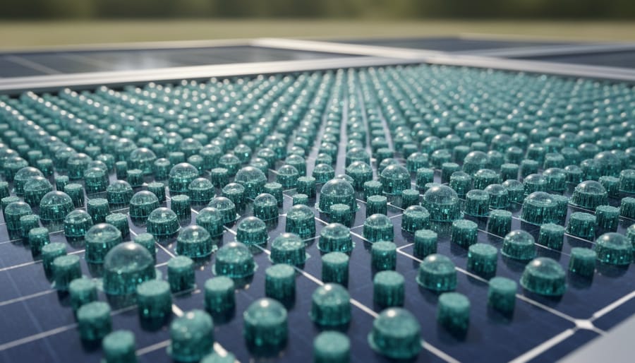
Light-trapping structures represent one of 2PP’s most valuable contributions. The technology produces intricate three-dimensional patterns featuring pyramidal textures, inverted cones, and nano-pillar arrays that increase the optical path length within solar cells. These structures reduce reflection losses by redirecting incident light into the absorber layer multiple times, allowing thinner cells to capture more photons effectively. Research collaborations between industry and universities have demonstrated reflection reductions exceeding 95 percent across broad spectral ranges.
Anti-reflective surfaces manufactured through 2PP employ biomimetic designs inspired by moth-eye structures. These gradual refractive index transitions minimize interface reflections more effectively than traditional thin-film coatings, particularly at oblique angles where standard panels lose efficiency. The sub-wavelength features create smooth optical transitions that remain effective throughout daily sun movement.
Micro-lens arrays fabricated via 2PP concentrate incoming light onto active cell areas while directing it away from inactive grid lines and contact regions. These precisely engineered lenses, with diameters ranging from 10 to 100 micrometers, achieve customized focal lengths and numerical apertures optimized for specific cell architectures. Educational programs now incorporate 2PP-based optical design to prepare the next generation of photovoltaic engineers for implementing these advanced light management solutions in commercial production.
Electrode Pattern Optimization
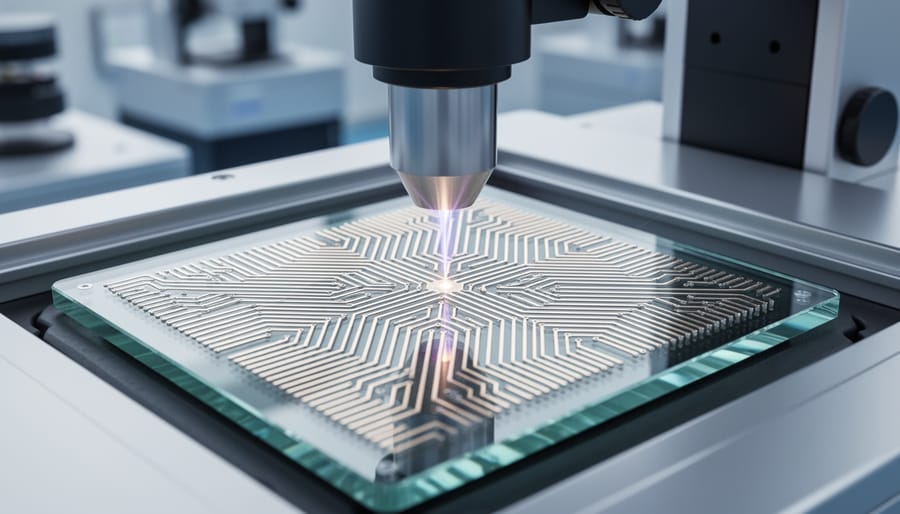
Two-photon polymerization 3D printing enables unprecedented precision in creating electrode patterns for photovoltaic cells, addressing one of the most persistent challenges in solar panel efficiency: shadowing losses. Traditional screen-printed electrodes typically occupy 6-10% of the cell’s front surface, blocking valuable sunlight from reaching the photovoltaic material. With 2PP technology, manufacturers can produce ultra-fine electrode patterns with line widths below 20 micrometers, reducing this shadowing effect by up to 40% compared to conventional methods.
The precision of 2PP printing allows engineers to optimize the balance between electrical conductivity and optical transparency. By creating taller, narrower electrode fingers with precisely controlled aspect ratios, current collection improves while maintaining minimal surface coverage. Research conducted in collaboration with universities has demonstrated that these optimized patterns can increase overall cell efficiency by 0.5-1.2 percentage points, a significant improvement in an industry where every fraction matters.
Additionally, 2PP technology enables the fabrication of complex three-dimensional contact geometries that enhance adhesion and reduce contact resistance. The technique permits direct writing of conductive polymer structures that can be subsequently metallized, creating robust electrical connections without the thermal stress associated with traditional firing processes. This capability proves particularly valuable for advanced cell architectures like heterojunction and PERC designs, where temperature sensitivity limits conventional metallization approaches. Educational program offerings increasingly incorporate these advanced manufacturing techniques, preparing the next generation of photovoltaic professionals to leverage additive manufacturing for enhanced solar cell performance.
Protective Coatings and Encapsulation Structures
Two-photon polymerization 3D printing enables the creation of sophisticated protective coatings and encapsulation structures that significantly extend solar panel lifespan. By fabricating nano-structured barriers with precise architectmic control, manufacturers can develop next-generation protection systems that outperform conventional encapsulation methods.
The technology produces ultra-thin polymer layers featuring tailored surface topographies at the nanoscale. These engineered surfaces enhance water repellency, reduce particle adhesion, and minimize light-induced degradation of underlying photovoltaic materials. Research collaborations between industry leaders and universities have demonstrated that 2PP-fabricated protective layers can incorporate hierarchical structures mimicking natural hydrophobic surfaces, such as lotus leaves, achieving superior self-cleaning properties essential for maintaining optimal panel efficiency.
Advanced encapsulation designs created through 2PP address critical failure mechanisms in solar modules. The technique allows fabrication of microscale barriers with strategic stress-relief features that accommodate thermal expansion mismatches between different panel components. These structures prevent delamination and moisture ingress, two primary causes of long-term performance degradation. Studies indicate that panels incorporating 2PP-enhanced encapsulation demonstrate improved resistance to potential-induced degradation and reduced degradation rates under accelerated aging tests.
Educational programs focusing on protective coating development increasingly incorporate 2PP methodologies, recognizing their importance for future manufacturing innovation. The ability to prototype and test novel encapsulation geometries rapidly accelerates material science research, enabling optimization of protective systems before scaling to commercial production. This technology particularly benefits emerging photovoltaic technologies requiring specialized protection strategies, including perovskite solar cells and organic photovoltaics, where conventional encapsulation approaches prove inadequate for ensuring commercial viability and extended operational lifetimes.
Efficiency Gains and Performance Improvements
The integration of two-photon polymerization 3D printing into solar photovoltaic manufacturing has demonstrated measurable efficiency gains across multiple performance parameters. Recent research collaborations between industry partners and academic institutions have documented significant improvements that validate the commercial viability of this advanced manufacturing approach.
A landmark 2022 study conducted jointly by the Karlsruhe Institute of Technology and Fraunhofer ISE examined silicon heterojunction solar cells enhanced with 2PP-fabricated microstructures. The research team reported absolute efficiency increases of 1.8 to 2.3 percentage points compared to conventional cells. This improvement resulted primarily from optimized light management through precisely engineered surface texturing that reduced reflection losses from 8.5% to under 3%. The microstructured patterns, featuring dimensions between 2 and 10 micrometers, enabled superior light trapping across the entire solar spectrum while maintaining excellent passivation properties.
Performance testing of perovskite solar modules incorporating 2PP-printed charge transport layers revealed enhanced operational stability alongside efficiency gains. Researchers at the Swiss Federal Institute of Technology documented power conversion efficiencies reaching 24.7% in laboratory conditions, with accelerated aging tests showing only 12% degradation after 1,000 hours under standard testing protocols. This represents a substantial improvement over comparable modules using conventional deposition methods, which typically exhibit 18-22% degradation under identical conditions.
Field trials conducted across diverse geographic locations have validated laboratory findings. A twelve-month deployment study in Arizona examined bifacial modules featuring 2PP-enhanced rear-side optical structures. The modified modules generated 8.3% more energy annually compared to standard bifacial designs, with particularly pronounced gains during morning and evening hours when incident light angles typically reduce performance.
Manufacturing efficiency has also improved through 2PP integration. Industrial partners report reduced material waste of approximately 35% compared to subtractive manufacturing processes, as the additive approach deposits material only where needed. Process cycle times for creating complex microstructures decreased from hours to minutes, enabling higher throughput for specialized component production.
These documented improvements demonstrate that two-photon polymerization technology delivers tangible performance advantages in solar applications, supporting its continued development and commercialization within the photovoltaic industry.
Current Limitations and Manufacturing Challenges
Despite its remarkable precision, two-photon polymerization 3D printing faces substantial hurdles that currently limit its widespread adoption in photovoltaic manufacturing. Understanding these constraints is essential for industry stakeholders evaluating this technology’s near-term commercial potential.
Production speed remains the most significant bottleneck. Two-photon polymerization operates at micrometer and nanometer scales, requiring the laser focal point to trace each structural feature sequentially. This point-by-point writing process translates to fabrication speeds measured in cubic millimeters per hour rather than the cubic centimeters achieved by conventional manufacturing methods. For solar cell component production requiring large surface areas, these throughput limitations create serious scalability concerns that must be addressed before industrial-scale implementation becomes economically viable.
Cost considerations present another major barrier. Commercial two-photon polymerization systems typically range from $200,000 to over $500,000, excluding specialized photoresins and ongoing maintenance expenses. The femtosecond lasers central to the process demand precise environmental controls and skilled operators, adding to operational overhead. These capital and operating costs currently restrict two-photon polymerization primarily to research institutions and specialized applications where the precision justifies the investment.
Material availability poses additional challenges. The photoresins compatible with two-photon polymerization represent a limited subset compared to materials used in traditional photovoltaic manufacturing. Most commercially available photoresins are polymer-based, requiring additional metallization or composite integration steps to achieve the electrical conductivity needed for functional solar cell components. Developing photoresins with embedded metallic nanoparticles or semiconducting properties remains an active research area with promising but incomplete results.
The gap between laboratory demonstrations and commercial viability remains substantial. While academic research consistently showcases impressive efficiency improvements in small-scale prototypes, translating these results to production-scale manufacturing introduces complexities involving process reliability, quality control protocols, and integration with existing fabrication workflows. Universities collaborating with industry partners are working to bridge this gap, but significant development timelines and validation testing separate current capabilities from market-ready solutions that meet the demanding reliability standards photovoltaic installations require.
The Path to Commercial Adoption
University Research and Educational Initiatives
Leading academic institutions worldwide are establishing specialized programs to advance two-photon polymerization technology and prepare future photovoltaic professionals for this emerging field. Universities such as MIT, Karlsruhe Institute of Technology, and the Technical University of Vienna have integrated 2PP training into their materials science and renewable energy curricula, providing students with hands-on experience in nanoscale additive manufacturing.
These educational initiatives typically combine theoretical coursework in nonlinear optics and polymer chemistry with practical laboratory sessions using commercial 2PP systems. Students learn to design and fabricate microstructured components relevant to solar energy applications, from light-trapping architectures to advanced electrode patterns. Research collaborations between universities and solar manufacturers enable students to work on real-world challenges, such as optimizing absorption efficiency through precision nanostructuring.
Several institutions have established dedicated research centers focusing on 2PP applications in photovoltaics, offering graduate programs and industry partnerships that bridge the gap between laboratory innovation and commercial implementation. This academic foundation ensures a pipeline of skilled professionals capable of advancing 2PP technology within the renewable energy sector, accelerating its transition from experimental technique to industrial manufacturing standard.

Industry Investment and Pilot Programs
Several forward-thinking companies are integrating two-photon polymerization into photovoltaic research and development initiatives. Nanoscribe, a leader in 2PP technology, has partnered with solar research institutions to develop pilot programs focused on microscale light management structures for solar cells. Their collaboration with the Fraunhofer Institute for Solar Energy Systems has produced promising prototypes demonstrating enhanced absorption efficiency.
Leading solar manufacturers including LONGi and JinkoSolar have established dedicated additive manufacturing research divisions exploring 2PP applications for next-generation panel designs. These pilot programs primarily focus on creating advanced anti-reflective surface textures and optimized light-trapping geometries at the nanoscale level.
Academic partnerships play a crucial role in advancing 2PP adoption. MIT’s Photovoltaic Research Laboratory and Stanford’s Center for Advanced Molecular Photovoltaics are conducting extensive studies on 2PP-fabricated micro-concentrator systems. These educational collaborations combine theoretical research with practical manufacturing trials, training the next generation of photovoltaic engineers in advanced fabrication techniques.
Early adoption efforts concentrate on high-efficiency specialty applications rather than mass production, with 2PP joining other revolutionary solar technologies being tested for commercial viability. Investment levels remain modest but growing, with industry analysts projecting increased funding as manufacturing costs decline.
What This Means for PV Professionals
The integration of two-photon polymerization 3D printing into photovoltaic manufacturing represents a significant shift that demands new competencies from industry professionals. Those working in or entering the solar energy sector should recognize this technology as both an opportunity and a call to expand their skill sets.
Current and aspiring PV professionals will benefit from developing expertise in additive manufacturing processes, particularly precision microfabrication techniques. Understanding the principles of 2PP technology, including its laser-based polymerization methods and nanoscale precision capabilities, will become increasingly valuable. While strong foundations in photovoltaic technology fundamentals remain essential, cross-disciplinary knowledge bridging traditional PV engineering with advanced manufacturing will distinguish leading professionals.
Career opportunities are emerging in several areas. Research and development positions focused on optimizing 2PP applications for solar components are expanding at universities and private laboratories. Manufacturing engineering roles requiring expertise in implementing and maintaining 2PP systems are appearing as early adopters scale production. Quality assurance specialists who understand both PV performance metrics and additive manufacturing tolerances will be in high demand.
To prepare for this technological evolution, professionals should pursue continuing education in advanced manufacturing techniques and materials science. Many universities now offer specialized courses and certificate programs in additive manufacturing for energy applications. Participating in industry conferences, joining professional organizations focused on solar innovation, and staying current with peer-reviewed research will provide competitive advantages.
Hands-on experience, even with more accessible 3D printing technologies, builds transferable knowledge about layer-by-layer fabrication principles. Collaboration between academia and industry creates pathways for professionals to engage with cutting-edge 2PP research while contributing practical manufacturing insights. Those who proactively develop these competencies position themselves at the forefront of solar technology advancement.
Two-photon polymerization 3D printing represents a transformative advancement for solar photovoltaic manufacturing, offering unprecedented precision in creating nanoscale features that significantly enhance light absorption, carrier collection, and overall module efficiency. As this article has demonstrated, 2PP technology enables the fabrication of optimized surface textures, anti-reflective structures, and innovative grid designs that push the boundaries of what conventional manufacturing can achieve.
However, aspiring professionals and industry stakeholders must maintain realistic expectations regarding implementation timelines. While laboratory demonstrations have proven the technology’s potential, transitioning from research environments to high-volume production facilities will require substantial investment in infrastructure, process optimization, and quality control systems. Industry experts project that widespread commercial adoption may take five to ten years, with initial applications likely focusing on premium products and specialized applications where the performance gains justify higher manufacturing costs.
The path forward depends critically on continued education and collaborative innovation. Universities and research institutions play an essential role in advancing 2PP techniques, developing novel photoresist materials, and training the next generation of photovoltaic professionals who understand both additive manufacturing principles and solar cell physics. Educational programs that bridge these disciplines will be instrumental in accelerating technology maturation.
For renewable energy enthusiasts and environmentally conscious consumers, 2PP represents more than manufacturing innovation—it embodies the commitment to pushing efficiency boundaries that make solar energy increasingly competitive and accessible. By staying informed about emerging technologies and supporting research initiatives, stakeholders across the solar industry can contribute to realizing 2PP’s full potential in mainstream photovoltaic production.