The evolution of photovoltaic cell production represents one of modern manufacturing’s most sophisticated achievements, combining precision engineering with cutting-edge materials science. From silicon purification to module assembly, this intricate process transforms raw materials into high-efficiency solar panels that power our renewable energy future. Recent technological breakthroughs, including automated production lines and advanced quality control systems, have revolutionized manufacturing efficiency while dramatically reducing costs. Industry leaders now achieve conversion efficiencies exceeding 23% in mass production, marking a significant leap forward in sustainable energy technology. Understanding these manufacturing processes is crucial for stakeholders across the renewable energy sector, from engineers and investors to environmental policy makers, as global demand for solar technology continues its exponential growth.
This article examines the step-by-step journey of photovoltaic manufacturing, highlighting innovative techniques, quality control measures, and emerging technologies that are reshaping the industry’s landscape. We’ll explore how modern facilities combine traditional manufacturing principles with artificial intelligence and automation to produce solar panels that are more efficient, durable, and cost-effective than ever before.
Raw Material Processing and Silicon Preparation
Silicon Purification
Silicon purification is a critical step in photovoltaic manufacturing, transforming raw silicon into solar-grade material with purity levels exceeding 99.9999%. The process begins with metallurgical-grade silicon (98% pure), which undergoes several refinement stages to achieve the required purity for solar applications.
The primary purification method is the Siemens process, where trichlorosilane gas (SiHCl3) is produced by reacting metallurgical-grade silicon with hydrochloric acid. This gas is then heated to temperatures around 1100°C in the presence of hydrogen, resulting in the deposition of high-purity polycrystalline silicon on silicon seed rods.
An alternative method gaining prominence is the fluidized bed reactor (FBR) process, which offers reduced energy consumption and lower production costs. In FBR, silicon particles are suspended in a reactive gas mixture, allowing continuous deposition of pure silicon while maintaining efficient heat transfer.
The refined silicon then undergoes directional solidification or the Czochralski process to form ingots suitable for solar cell production. These methods further reduce impurities and establish the desired crystal structure. Quality control measures, including resistivity testing and chemical analysis, ensure the silicon meets solar-grade specifications.
Modern purification techniques increasingly focus on sustainable practices, incorporating recycled silicon and optimizing energy consumption while maintaining the strict purity requirements essential for efficient solar cell performance.
Ingot and Wafer Production
The production of silicon ingots and wafers represents a crucial phase in photovoltaic manufacturing. The process begins with high-purity silicon feedstock, which undergoes careful melting and crystallization to form mono and multi-crystalline silicon ingots.
For monocrystalline ingots, manufacturers employ the Czochralski method, where a seed crystal is dipped into molten silicon and slowly pulled upward while rotating. This technique produces a cylindrical ingot with a uniform crystal structure, resulting in higher efficiency solar cells. The process requires precise temperature control and clean room conditions to ensure optimal crystal formation.
Multicrystalline ingots are produced through directional solidification, where molten silicon is cooled gradually in a crucible. This method is more cost-effective but yields ingots with multiple crystal boundaries, slightly reducing their efficiency potential.
Once the ingots are formed, they undergo wire sawing to create thin wafers, typically 150-180 micrometers thick. Diamond-coated wire saws slice through the ingots with high precision while minimizing material waste. The wafers are then cleaned, textured, and inspected for defects before moving to the cell manufacturing phase. Advanced automation systems and quality control measures ensure consistent wafer production while maintaining the strict tolerances required for solar cell fabrication.

Cell Manufacturing Technologies
Surface Texturing and Cleaning
Surface texturing and cleaning are critical steps in photovoltaic wafer preparation that significantly impact solar cell efficiency. The process begins with chemical etching, typically using a combination of sodium hydroxide or potassium hydroxide solutions, which creates microscopic pyramidal structures on the wafer surface. These structures reduce light reflection and increase photon absorption by allowing multiple opportunities for light to enter the cell.
Following texturing, wafers undergo a rigorous cleaning sequence to remove contaminants, organic residues, and metal impurities. This usually involves a multi-step process using various chemical solutions, including hydrochloric acid, hydrofluoric acid, and hydrogen peroxide mixtures. The industry-standard RCA cleaning method, developed by Radio Corporation of America, remains widely used for its effectiveness in removing specific types of contaminants.
Advanced cleaning technologies, such as ultrasonic cleaning systems and automated handling equipment, ensure consistent results while minimizing wafer breakage. Quality control measures, including surface roughness measurements and contamination monitoring, are performed throughout these processes to maintain manufacturing standards and optimize cell performance.

Doping and Junction Formation
The doping and junction formation process is crucial in creating the photovoltaic effect within solar cells. After silicon purification, manufacturers introduce specific impurities (dopants) into the silicon wafer through either thermal diffusion or ion implantation methods. The most common dopants are boron for p-type regions and phosphorus for n-type regions.
Thermal diffusion involves exposing silicon wafers to dopant-rich gases at temperatures between 800°C and 1000°C. The dopant atoms diffuse into the silicon crystal structure, creating the necessary charge carriers. Ion implantation, a more precise alternative, uses accelerated dopant ions directed at the silicon surface, allowing for better control of junction depth and dopant concentration.
The formation of the P-N junction occurs at the interface between differently doped regions. This junction is essential for charge separation when the cell is exposed to sunlight. Modern manufacturing facilities often employ automated systems with precise temperature and atmospheric controls to ensure consistent junction formation across thousands of wafers simultaneously, maximizing production efficiency while maintaining quality standards.
Anti-reflection Coating Application
Anti-reflection coating (ARC) plays a crucial role in maximizing the efficiency of photovoltaic cells by reducing light reflection from the silicon surface. The most common technique involves plasma-enhanced chemical vapor deposition (PECVD) to apply a thin layer of silicon nitride, typically 70-80 nanometers thick. This blue-purple coating not only minimizes reflection but also provides surface passivation, reducing electron-hole recombination.
The application process begins with surface cleaning and preparation, followed by the controlled deposition of the anti-reflective material in a vacuum chamber. The silicon wafer is heated to approximately 400°C while precise amounts of silane (SiH4) and ammonia (NH3) gases are introduced. Through plasma activation, these gases react to form the silicon nitride coating, which adheres uniformly to the cell surface.
Modern manufacturing facilities often employ inline PECVD systems that can process multiple wafers simultaneously, significantly increasing production throughput. Quality control measures, including spectral reflectance testing and thickness uniformity checks, ensure optimal coating performance. This process typically reduces surface reflection from over 30% to less than 4%, substantially improving the cell’s light absorption capabilities.
Metallization and Contact Formation
Metallization and contact formation represents a crucial step in photovoltaic cell manufacturing, where electrical contacts are created to collect and transport the generated electricity. The process typically involves screen printing of metal pastes, predominantly silver for the front contacts and aluminum for the rear surface. The front contact pattern consists of thin finger lines connected to wider bus bars, optimized to minimize shading while maximizing electrical conductivity.
Advanced metallization techniques include electroplating, physical vapor deposition (PVD), and copper-based alternatives to reduce dependency on costly silver. The printed metal contacts undergo a high-temperature firing process, typically between 700-900°C, to ensure proper contact formation and adhesion to the silicon surface. This thermal treatment also facilitates the formation of a back surface field through aluminum alloying, which enhances cell efficiency.
Quality control during metallization is essential, as contact resistance and adhesion strength directly impact cell performance. Modern manufacturing lines employ automated optical inspection systems and electrical testing to verify contact integrity and pattern accuracy. Recent innovations focus on reducing metal paste consumption while maintaining or improving cell efficiency through techniques like selective emitter formation and fine-line printing.
Advanced Manufacturing Innovations
PERC Technology Implementation
PERC technology implementation represents a significant advancement in solar cell manufacturing, offering enhanced efficiency through sophisticated rear surface engineering. The process begins with the application of a dielectric passivation layer to the rear surface of conventional solar cells, typically using aluminum oxide (Al2O3) deposited through atomic layer deposition (ALD) or plasma-enhanced chemical vapor deposition (PECVD).
Following passivation, laser ablation creates microscopic openings in the dielectric layer, allowing for selective contact formation between the aluminum back surface field and the silicon wafer. This step optimizes electron flow while minimizing recombination losses. The subsequent metallization process involves screen-printing aluminum paste onto the rear surface, which, during the firing step, forms local contacts through the ablated openings.
The final stages include edge isolation and testing to ensure optimal performance. The entire PERC manufacturing process typically adds only 2-3 steps to conventional cell production while delivering efficiency gains of 1-2% absolute. Modern manufacturing lines can achieve throughput rates of over 6,000 wafers per hour while maintaining consistent quality and performance metrics. This advanced process has become the industry standard due to its cost-effectiveness and significant performance improvements over traditional cell architectures.
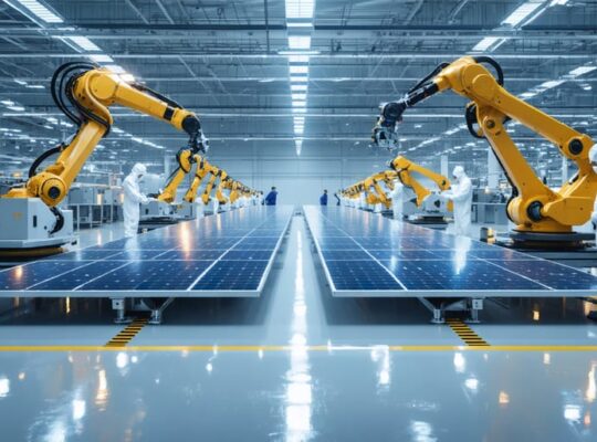
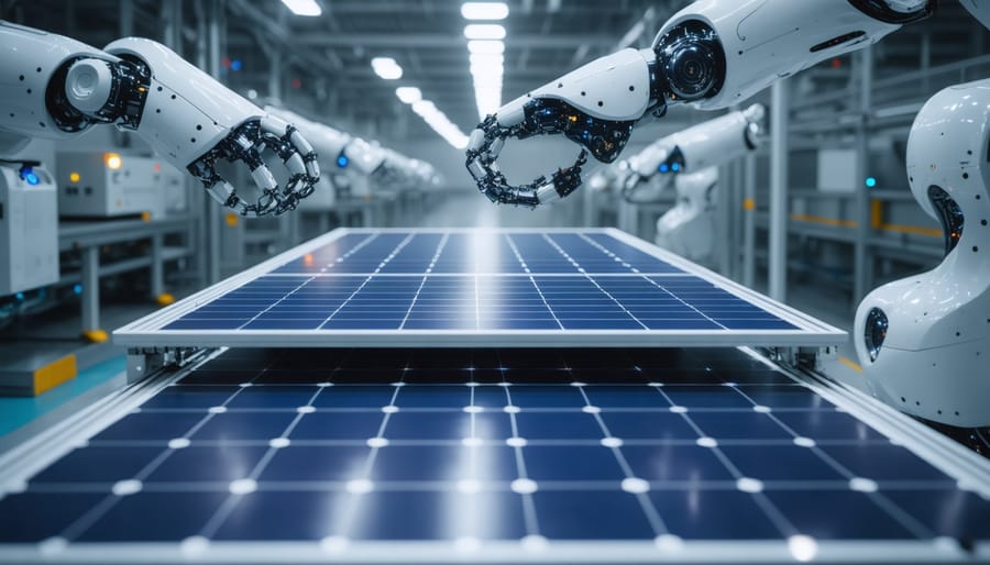
Automated Quality Control
Modern photovoltaic manufacturing relies heavily on automated quality control systems to maintain consistent product excellence. These sophisticated inspection methods combine machine vision technology, artificial intelligence, and precision sensors to detect defects throughout the production process.
Electroluminescence (EL) imaging serves as a primary inspection technique, capturing detailed images of cells to identify micro-cracks, broken connections, and other internal defects that might be invisible to the naked eye. This non-destructive testing method ensures thorough examination without compromising the integrity of the modules.
Advanced thermal imaging systems monitor heat distribution patterns across panels, identifying potential hot spots and circulation issues before they become problematic. Meanwhile, specialized IV curve testing equipment measures electrical performance parameters, ensuring each module meets strict efficiency standards.
In-line monitoring systems continuously track key metrics during production, including material thickness, coating uniformity, and cell alignment. Any deviations from prescribed specifications trigger immediate alerts, allowing for real-time adjustments and minimizing waste.
Data from these quality control processes is automatically logged and analyzed using advanced analytics platforms, enabling manufacturers to identify trends, optimize production parameters, and maintain consistent quality standards across large-scale operations. This comprehensive approach to quality control has significantly improved manufacturing yield rates while reducing defect-related warranty claims.
Industry 4.0 Integration
The integration of Industry 4.0 technologies has revolutionized photovoltaic manufacturing, bringing unprecedented levels of automation, precision, and efficiency to the production process. Smart manufacturing systems now incorporate artificial intelligence and machine learning algorithms to optimize production parameters in real-time, resulting in higher cell efficiencies and reduced waste.
Advanced sensor networks throughout the production line continuously monitor critical parameters such as temperature, pressure, and material composition. This data feeds into sophisticated manufacturing execution systems (MES) that provide comprehensive visibility and control over the entire production process. The implementation of digital twins enables manufacturers to simulate and optimize production scenarios before actual implementation.
Industrial Internet of Things (IIoT) devices facilitate seamless communication between different manufacturing equipment, while big data analytics help identify patterns and predict potential issues before they affect production quality. Predictive maintenance systems analyze equipment performance data to schedule maintenance activities proactively, reducing unexpected downtime and extending machinery lifespan.
Quality control has been enhanced through computer vision systems and AI-powered inspection tools that can detect microscopic defects with greater accuracy than traditional methods. These systems can automatically adjust process parameters to maintain optimal production conditions and ensure consistent product quality.
The adoption of Industry 4.0 principles has also improved supply chain management through real-time inventory tracking and demand forecasting, enabling just-in-time manufacturing and reducing storage costs while maintaining production efficiency.
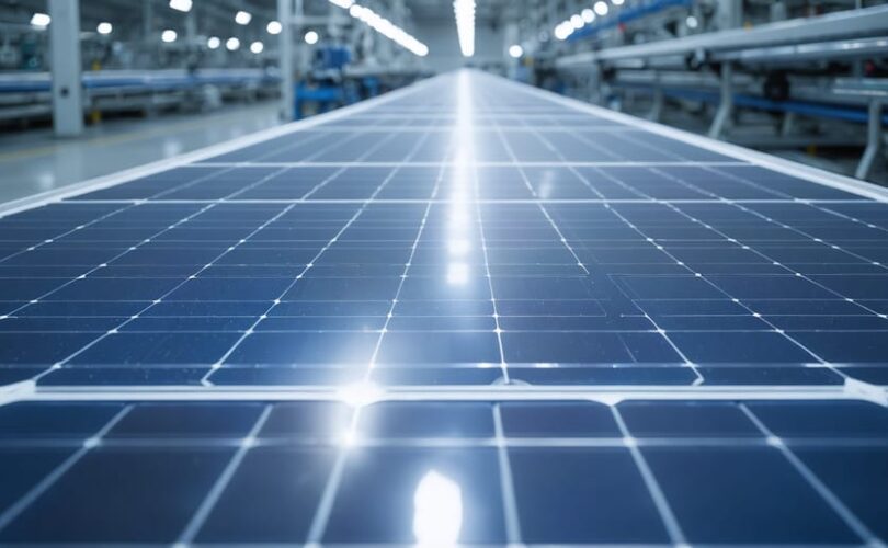
Module Assembly and Testing
Cell Stringing and Layup
Cell stringing and layup represents a critical phase in photovoltaic module assembly where individual solar cells are electrically connected and arranged in a specific pattern. During this process, solar cells are connected in series using copper ribbons, typically through automated soldering equipment that precisely applies heat and pressure to create reliable electrical connections.
The cells are arranged in strings, with the number of cells determined by the desired voltage output of the final module. Modern manufacturing facilities employ advanced robotics and computer vision systems to ensure precise placement and consistent spacing between cells. These systems can detect microscopic defects or misalignments that could affect module performance.
Once the cells are connected in strings, they are arranged in a matrix configuration on a sheet of encapsulant material, usually EVA (Ethylene Vinyl Acetate). The layout pattern is carefully calculated to maximize power output while maintaining the module’s dimensional requirements. Multiple strings are connected in parallel using bus bars to achieve the desired current specifications.
Quality control measures during this stage include electrical testing of individual strings, visual inspection for proper alignment, and verification of solder joint integrity. Advanced manufacturers utilize electroluminescence imaging to detect any micro-cracks or connection issues before proceeding to the lamination stage. This careful attention to detail during cell stringing and layup is essential for ensuring the long-term reliability and performance of the finished photovoltaic module.
Lamination and Framing
Lamination and framing represent crucial final steps in photovoltaic module manufacturing, ensuring long-term durability and environmental protection. The process begins with the careful layering of materials: the solar cell strings are sandwiched between sheets of EVA (ethylene-vinyl acetate) encapsulant, with a tempered glass cover on top and a protective backsheet on the bottom.
These layers undergo lamination in specialized machines under controlled temperature and pressure conditions, typically between 140-160°C. During this process, the EVA melts and flows around the solar cells, creating an airtight seal that prevents moisture ingress and provides structural support. The lamination process usually takes 15-20 minutes to complete, during which vacuum conditions ensure no air bubbles remain trapped between layers.
After lamination, the module edges are trimmed and cleaned before aluminum frames are attached. The frames serve multiple purposes: they provide structural rigidity, facilitate mounting, and protect the module edges from impact damage. A specialized silicone sealant is applied between the frame and laminate to ensure weatherproof connections.
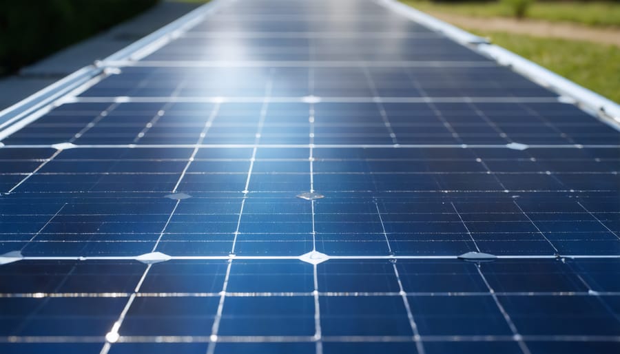
Junction boxes are then attached to the module’s backside, housing the bypass diodes and providing connection points for the electrical cables. The completed modules undergo rigorous quality testing, including electrical performance verification, mechanical load testing, and visual inspection, before receiving final certification for deployment.
The photovoltaic manufacturing industry has undergone significant transformation in recent years, driven by technological advancements, increased automation, and growing demand for sustainable energy solutions. Manufacturing processes have become more efficient and cost-effective, leading to substantial reductions in solar panel production costs and improved product quality.
Current trends indicate a shift toward higher efficiency cell technologies, including the adoption of PERC, heterojunction, and tandem cell architectures. Industry leaders are increasingly investing in smart manufacturing facilities that incorporate artificial intelligence, machine learning, and advanced process control systems to optimize production yields and reduce waste.
The future outlook for PV manufacturing appears promising, with continued innovation expected in materials science, production techniques, and quality control methods. Emerging technologies such as perovskite solar cells and advanced thin-film processes are showing potential to revolutionize the industry further. Additionally, there is a growing focus on sustainable manufacturing practices, including reduced water consumption, improved material recycling, and lower carbon footprints.
Challenges remain in scaling up production while maintaining quality standards and managing supply chain complexities. However, ongoing research collaborations between industry and academia are addressing these challenges through innovative solutions and process improvements. The industry is also witnessing increased regionalization of manufacturing capabilities, reducing dependency on single-source markets and strengthening global supply chain resilience.
As the world continues its transition toward renewable energy, PV manufacturing will play a crucial role in meeting the growing demand for solar panels. With continued technological advancement and process optimization, the industry is well-positioned to support the global shift toward sustainable energy production while maintaining competitive costs and high-quality standards.