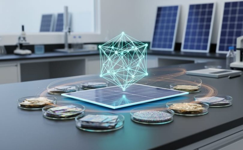
AI-powered materials discovery accelerates the identification of high-performance photovoltaic materials by 50 to 100 times compared to conventional laboratory methods, transforming what once required decades of trial-and-error experimentation into targeted campaigns that can be completed in months. Machine learning algorithms trained on existing materials databases can predict promising candidate compounds, simulate their electronic and optical properties, and prioritize those most likely to achieve target efficiency thresholds before a single physical sample enters the lab.
The approach combines computational screening, predictive modeling, and experimental validation in an iterative workflow. Rather than synthesizing and testing thousands of material variants manually, researchers now define target properties (bandgap, stability, toxicity limits), train algorithms on crystallographic and performance data, and generate ranked lists of candidates worth fabricating. This methodology has already contributed to breakthroughs in perovskite compositions, earth-abundant absorber layers, and transparent conducting oxides, expanding the solar PV benefits accessible to manufacturers and end users alike.
Success requires cross-disciplinary expertise. Materials scientists collaborate with data engineers to curate training datasets, while computational chemists validate AI predictions through density functional theory calculations before experimental teams synthesize top candidates. At Moser Baer Solar, our partnerships with leading universities integrate these techniques into educational programs, preparing the next generation of photovoltaic professionals to work fluently across computational and laboratory environments. The process is iterative, not automatic, and demands careful validation at each stage to distinguish genuine innovations from algorithmic artifacts.
Tools and Platforms Required for AI Materials Discovery
Computational Infrastructure and Hardware
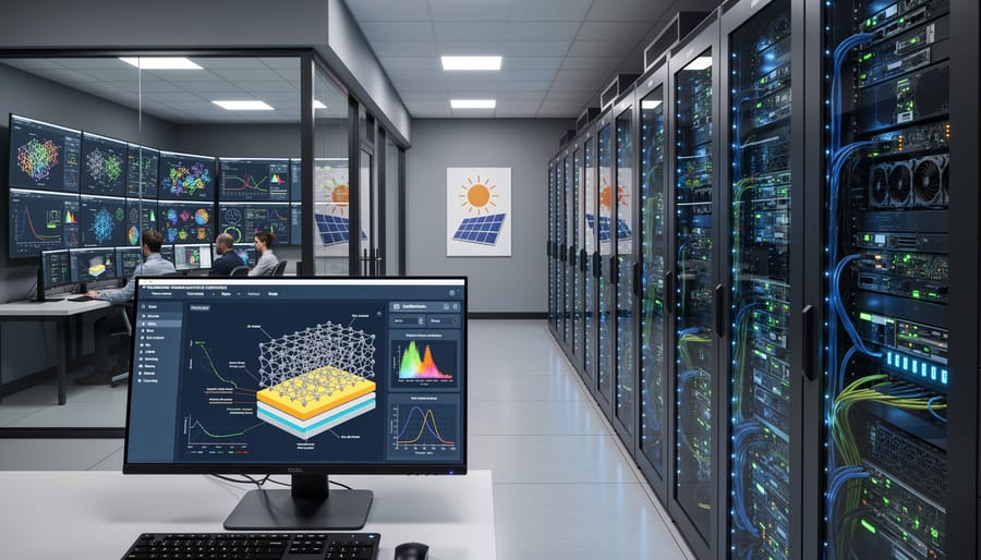
Running AI-driven materials discovery for solar PV demands substantial computing power. Your infrastructure choices directly impact simulation speed, model training time, and research throughput.
For local workstations, plan for high-performance GPUs, NVIDIA A100 or RTX 4090 cards provide the parallel processing essential for training neural networks on crystal structures and material properties. Pair these with at least 64GB RAM and fast NVMe storage for handling large datasets from materials databases. A dual-GPU setup accelerates both model training and density functional theory calculations, cutting weeks-long simulations to days.
Cloud platforms offer scalable alternatives without upfront capital investment. AWS EC2 P4 instances and Google Cloud’s A2 machine types deliver enterprise-grade GPU access on demand. These services charge by the hour, making them cost-effective for burst workloads like screening thousands of material candidates. You can spin up 10 instances simultaneously during intensive discovery phases, then scale down for routine analysis.
Hybrid approaches work well for many research teams: use local workstations for model development and preliminary testing, then shift to cloud resources for large-scale screening campaigns. This balances cost control with computational flexibility as your discovery projects evolve.
Data Sources and Material Databases
Access to high-quality materials data forms the foundation of any successful AI discovery workflow. For solar PV applications, researchers need comprehensive databases that contain not just crystal structures but also the electronic and optical properties critical to photovoltaic performance.
Several open-source repositories provide essential starting points:
- Materials Project: Over 140,000 inorganic compounds with calculated band gaps, formation energies, and electronic structures
- NREL Materials Database: Experimental and computational data specifically for PV materials, including measured device performance
- Open Quantum Materials Database (OQMD): 815,000+ DFT-calculated thermodynamic and structural properties
- AFLOW: Automated computational framework with data on nearly 3 million materials and their properties
- Citrine Informatics Platform: Combines open and proprietary data with tools for materials informatics workflows
The most effective approach combines multiple databases to capture diverse material chemistries and property measurements. Collaboration with university research programs often provides access to specialized datasets from recent studies, including unpublished experimental results on emerging PV materials like perovskites, kesterites, and organic semiconductors. These partnerships, such as those fostered through Mose Solar’s educational initiatives, enable researchers to augment public data with cutting-edge findings that haven’t yet entered major repositories, significantly improving model training quality and prediction accuracy for novel material classes.
Safety and Compliance Warnings
Before deploying AI materials discovery workflows, understand the critical limitations and risks that can derail photovoltaic research efforts. Computational predictions are tools, not guarantees, and several factors demand careful attention to avoid costly missteps.
Data quality determines model reliability. Training datasets for PV materials often suffer from inconsistent measurement conditions, incomplete property reporting, and sampling bias toward well-studied material families. If your training data predominantly contains silicon and cadmium telluride examples with sparse representation of perovskites or emerging chemistries, the model will struggle to generalize. Validate dataset coverage against your target material space and document any gaps before investing compute resources.
Computational costs escalate quickly. A single high-throughput DFT validation campaign for 100 candidate materials can consume weeks of GPU cluster time and generate substantial cloud computing bills. Budget both the initial screening phase and iterative refinement cycles, recognizing that active learning approaches require multiple rounds.
Intellectual property becomes complex when AI generates novel compositions. Determine ownership rights before collaboration, especially when using proprietary training data or partnering with universities. Patent searches are essential since an AI-discovered material may already exist in prior art or be covered by existing claims, even if not widely synthesized.
Regulatory pathways for AI-discovered materials in commercial modules remain evolving. Novel absorber layers or encapsulants require extensive safety testing (toxicity, flammability, environmental impact) and certification by bodies like IEC 61215 standards for module qualification. Factor 18-24 months for regulatory approval after successful lab validation, particularly if the material contains elements not commonly used in existing PV products. Never assume computational stability predictions satisfy real-world durability requirements under UV exposure, thermal cycling, and humidity stress.
Step-by-Step Process for AI-Driven PV Materials Discovery
Step 1: Define Material Requirements and Target Properties
Before launching an AI discovery pipeline, you must translate your PV device goals into quantifiable material properties. Start by specifying the band gap: single-junction silicon alternatives typically need 1.1-1.7 eV to match the solar spectrum efficiently, while tandem cell components require narrower ranges depending on their position in the stack.
Next, define threshold values for absorption coefficient (>10⁴ cm⁻¹ in the visible range ensures adequate light harvesting), carrier mobility (>10 cm²/V·s for electrons and holes to minimize recombination losses), and minority carrier lifetime (>1 microsecond supports high open-circuit voltage). Stability constraints matter equally: materials must withstand 85°C and 85% humidity for 25+ years, resist UV degradation, and avoid toxic or scarce elements that inflate manufacturing costs.
Organize these criteria in a property target matrix with three columns: required (non-negotiable thresholds), desired (competitive advantages), and acceptable ranges (values your models will predict and filter against). This matrix becomes the evaluation rubric that guides model training, candidate screening, and ultimately determines which AI-predicted materials advance to computational validation.
Step 2: Assemble and Prepare Training Data
The foundation of effective AI materials discovery rests on assembling high-quality training data that represents known PV materials and their measured properties. Begin by extracting data from established repositories like the Materials Project, AFLOW, and OQMD, which provide computed properties for thousands of inorganic compounds including band gaps, formation energies, and crystal structures. Supplement computational databases with experimental measurements from peer-reviewed literature, particularly focusing on parameters critical to photovoltaics: absorption coefficients, carrier lifetimes, defect tolerance, and stability under operating conditions.
Data preparation requires meticulous cleaning to remove duplicates, outliers, and measurement errors. Standardize units across all sources (eV for band gaps, S/cm for conductivity), convert crystal structures to consistent formats (CIF or POSCAR), and verify that property measurements correspond to the same material phase and processing conditions. Address missing values strategically, exclude entries with incomplete target properties rather than imputing critical parameters like band gap or mobility.
The PV domain suffers from significant data gaps, particularly for emerging material classes like perovskites and organic semiconductors. Augment sparse datasets by incorporating closely related compositions, using symmetry operations to generate equivalent structures, and leveraging transfer learning from broader materials databases. Prioritize data quality over sheer volume: 500 rigorously validated measurements outperform 5,000 inconsistent entries when training predictive models for solar applications.
Step 3: Select and Train Appropriate AI Models
Selecting the right AI architecture is critical for accurate materials prediction. For solar PV applications, graph neural networks (GNNs) excel at learning from crystal structures because they naturally represent atoms as nodes and bonds as edges, capturing the three-dimensional geometry that determines electronic properties. Models like SchNet or CGCNN are proven choices for predicting band gaps and formation energies from atomic coordinates.
Deep neural networks work effectively for property prediction when you have tabular compositional data, elemental percentages, ionic radii, electronegativity values, as input features. Random forests often serve as strong baselines before moving to more complex architectures.
Genetic algorithms shine in composition optimization, particularly when exploring quaternary or quinary alloy spaces where you need to balance multiple competing properties: a wide band gap for voltage versus strong absorption for current generation.
Active learning strategies reduce the computational burden dramatically. Instead of screening millions of candidates blindly, the model identifies which materials would provide the most information if calculated next, iteratively refining predictions while minimizing expensive DFT calculations.
Training requires splitting your dataset into training, validation, and test sets, typically 70/15/15. Use cross-validation to prevent overfitting, especially with limited PV-specific data. Track metrics like mean absolute error for continuous properties and classification accuracy for categorical predictions like stability.
Step 4: Screen Material Candidates Through AI Predictions
With trained models ready, you can now execute large-scale screening campaigns that would be impossible through traditional experimental methods. Running predictions across millions of potential compositions allows systematic exploration of vast chemical spaces, reducing materials search times from years to weeks while identifying promising candidates that might never emerge from intuition-driven research.
Start by generating a comprehensive candidate library, typically 10⁴ to 10⁷ compositions depending on your search constraints. Your models rapidly predict key properties for each candidate: band gap, absorption coefficient, carrier mobility, and thermodynamic stability. This initial pass eliminates 95-99% of materials that fall outside target specifications for PV applications.
Apply a systematic filtering sequence to refine your candidate pool:
- Screen for target properties (band gap 1.1-1.7 eV, high absorption coefficient above 10⁴ cm⁻¹)
- Check thermodynamic stability using formation energy and decomposition pathway predictions
- Assess synthesizability through predicted synthetic accessibility scores and known precursor availability
- Filter for toxicity and environmental impact, prioritizing non-toxic materials and earth-abundant elements
- Evaluate cost implications based on raw material prices and processing complexity
- Select final candidates (10-50 materials) balancing predicted performance against practical constraints
Rank remaining candidates using a weighted scoring system that reflects your priorities, highest efficiency potential, lowest cost, fastest time-to-market, or best stability. This curated shortlist advances to computational validation, where you’ll verify predictions through rigorous first-principles calculations before committing resources to laboratory synthesis.
Step 5: Conduct High-Throughput Computational Validation
After screening thousands of potential materials, you need computational validation to confirm AI predictions before investing in laboratory synthesis. Density functional theory (DFT) calculations provide the rigorous verification required for photovoltaic materials.
Set up DFT simulations using software packages like VASP, Quantum ESPRESSO, or ABINIT to calculate fundamental properties with quantum mechanical precision. Focus your computational resources on the 10-50 top candidates identified during screening. Run band structure calculations to verify predicted band gaps and ensure appropriate semiconductor characteristics for solar absorption.
Calculate optical absorption spectra to confirm materials will efficiently capture sunlight across the relevant wavelength range. For PV applications, prioritize absorption coefficients above 10^4 cm^-1 in the visible spectrum. DFT simulations reveal whether materials exhibit direct or indirect band gaps, critical for device efficiency.
Examine defect formation energies to assess material stability and identify potential performance-limiting defects like vacancies or interstitials. Materials with low defect formation energies may suffer from recombination losses that reduce cell efficiency.
Model interface properties between your candidate absorber materials and common contact layers. Poor interface band alignment causes voltage losses that devastate device performance. This computational validation typically requires 2-4 weeks per material on adequate computing clusters, dramatically narrowing your experimental focus.
Step 6: Synthesize and Experimentally Test Promising Materials
Once computational validation confirms your top candidates, synthesize these materials in the laboratory using methods matching your target application. Thin film techniques like chemical vapor deposition (CVD), sputtering, or atomic layer deposition work well for absorber layers and transparent conductors, while solution processing methods (spin coating, inkjet printing) suit cost-sensitive or large-area applications. Start with small-scale samples, typically 1-5 cm² substrates, to minimize material waste and enable rapid iteration.
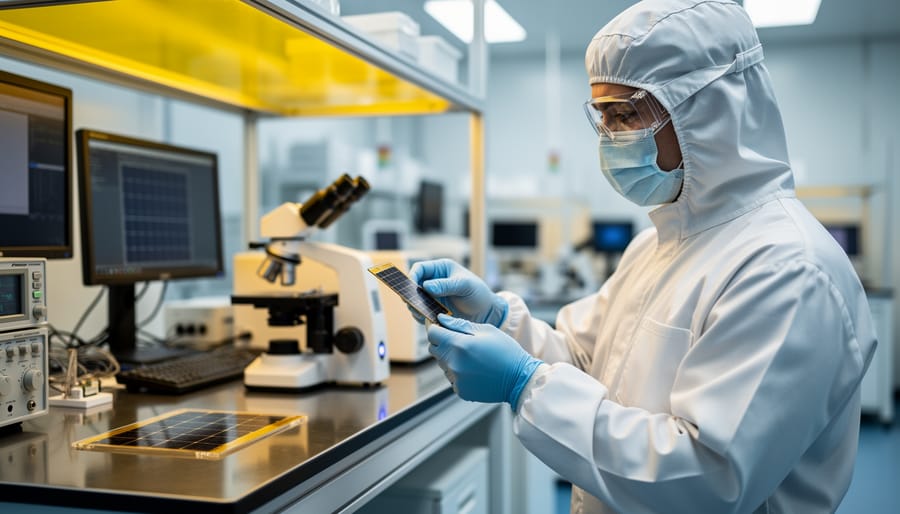
Characterize each synthesized material thoroughly before device integration. Use X-ray diffraction to verify crystal structure, spectroscopy (UV-Vis, photoluminescence) to measure optical properties, and scanning electron microscopy to examine morphology and grain boundaries. Hall effect measurements provide carrier mobility and doping concentration data critical for device performance prediction.
Fabricate test solar cells incorporating your novel materials, following established device architectures but substituting the AI-discovered material for the target layer. Measure current-voltage characteristics under standard AM1.5G illumination to determine conversion efficiency. Run accelerated stability tests (damp heat, UV exposure) to assess long-term viability. This experimental validation bridges the gap between computational predictions and advanced PV manufacturing confirming whether your discovered materials merit further development investment.
Verification, Analysis, and Next Steps
Measuring Discovery Success and Model Performance
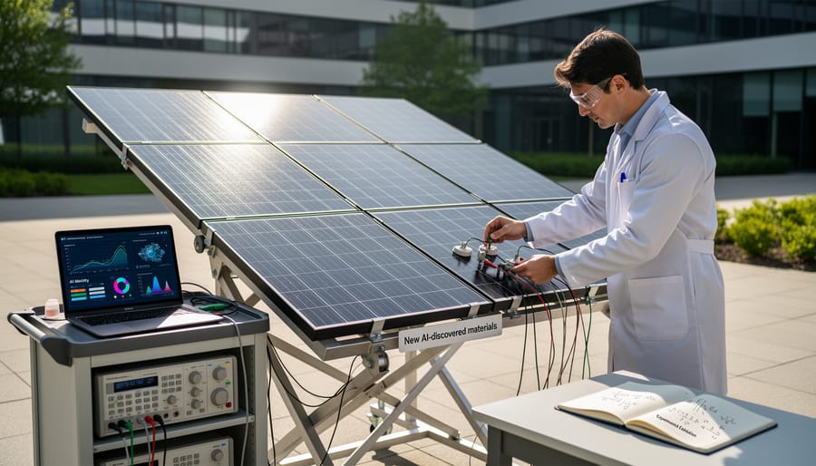
Evaluating your AI materials discovery pipeline requires tracking quantifiable metrics that demonstrate value beyond traditional experimental approaches. The most fundamental indicator is prediction accuracytypically measured through mean absolute error (MAE) for continuous properties like band gap or absorption coefficient. For PV applications, achieving MAE below 0.2 eV for band gap predictions represents strong model performance, while MAE above 0.5 eV suggests your model needs refinement or additional training data.
The discovery hit rate reveals practical impact, calculate the percentage of AI-predicted materials that experimentally meet your defined target properties. Traditional high-throughput screening achieves roughly 5-10% hit rates, whereas well-trained AI models regularly exceed 30-40% for established material classes. If your hit rate falls below 15%, investigate whether prediction errors, synthesizability issues, or misaligned target criteria are responsible.
Time-to-discovery metrics quantify efficiency gains. Track the duration from initial problem definition to validated candidates. Conventional materials development for PV absorbers typically spans 3-5 years, while AI-accelerated workflows compress this to 6-18 months when properly implemented. Document computational hours, experimental cycles required, and total researcher time invested. Compare these figures against historical benchmarks from similar projects to demonstrate ROI and justify continued investment in AI-driven discovery infrastructure.
Pathways from Discovery to Commercial PV Products
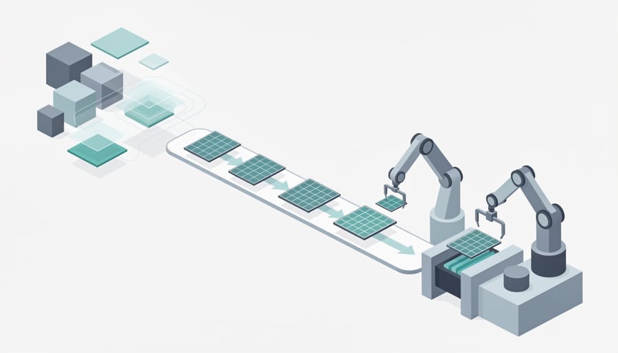
Once AI-guided materials validation confirms promising properties, bridging the gap to commercial deployment requires a structured scale-up pathway. Begin with synthesis scale-up trials, moving from milligram laboratory batches to kilogram pilot quantities, to identify process bottlenecks, refine deposition parameters, and establish reproducibility across larger substrate areas. At this stage, partner with university research programs and institutions like those supported by Mose Solar’s educational initiatives to access pilot-scale fabrication equipment and cross-validate results.
Parallel to synthesis development, initiate supply chain qualification by sourcing precursor materials in commercial quantities, evaluating supplier reliability, and assessing cost trajectories at volume. Simultaneously, engage with certification bodies early to understand testing requirements for high-efficiency PV modules including IEC 61215 qualification and long-term stability protocols under real-world conditions.
Integration into production lines demands compatibility assessments with existing module assembly processes and equipment. Conduct techno-economic analyses comparing performance gains against manufacturing cost increases, and explore licensing or joint development agreements with established PV manufacturers to leverage their infrastructure. Collaboration pathways through academic partnerships provide access to pilot lines, accelerate regulatory navigation, and train personnel in handling novel sustainable solar materials before full commercialization.
Common Questions About AI Materials Discovery in Solar PV
How long does AI materials discovery take compared to traditional methods?
AI-driven approaches typically reduce discovery timelines from 3-5 years to 6-18 months for new PV materials. The computational screening phase itself takes weeks rather than the years required for systematic experimental testing of all candidates, though experimental validation of promising materials still requires several months of lab work.
What level of expertise is needed to implement AI materials discovery?
Teams need a blend of materials science knowledge, machine learning skills, and computational chemistry expertise. Most successful implementations involve collaborations between PV researchers and data scientists, or training programs that develop hybrid skill sets, something universities and industry partnerships increasingly provide through specialized courses and workshops.
How accurate are AI predictions for photovoltaic materials?
Modern ML models achieve prediction accuracy within 0.1-0.3 eV for band gaps and 10-20% for properties like absorption coefficients when trained on quality data. However, accuracy varies significantly based on the specific property, training data quality, and how similar new candidates are to the training set, making experimental validation essential rather than optional.
Can small research groups or startups implement this approach?
Yes, though with some constraints. Cloud computing platforms and open-source tools have dramatically lowered barriers to entry, allowing small teams to access the necessary computational resources for a few hundred to a few thousand dollars per project. The main limitations are access to quality training data and the experimental facilities needed for synthesis and testing of predicted materials.
The cost question concerns many aspiring professionals evaluating whether to pursue this approach. Initial setup requires investment in computing infrastructure, either through cloud services or local GPU clusters, typically ranging from $5,000 to $50,000 depending on scale. Software licensing for commercial packages adds another cost layer, though open-source alternatives exist for most functions. The largest ongoing expense is often personnel, data scientists and materials researchers with the hybrid skill sets required command premium salaries in today’s competitive market.
Integration with existing research workflows actually proves more straightforward than many expect. AI materials discovery complements rather than replaces traditional experimental programs. Most successful groups maintain their core competencies in synthesis and characterization while adding computational screening as a front-end filter to prioritize experimental efforts. This hybrid approach allows researchers to leverage institutional knowledge and equipment investments while gaining efficiency through AI-guided exploration of chemical space.
Success stories in solar PV continue to accumulate. Research teams have used these methods to identify novel perovskite compositions with improved stability, discover earth-abundant alternatives to indium-based transparent conductors, and optimize multi-junction cell architectures. Several materials initially identified through AI screening have progressed to pilot-scale production. The track record demonstrates that computational predictions, when properly validated, translate into real device improvements, conversion efficiency gains of 1-3 percentage points in some cases, which represents substantial commercial value at scale.
AI materials discovery represents a fundamental shift in how we develop solar photovoltaic technologies. By compressing development timelines from years to months, these computational approaches accelerate the path toward higher-efficiency modules and lower-cost electricity generation. The researchers and manufacturers who master this workflow gain a competitive advantage in identifying the next breakthrough absorber, transparent conductor, or passivation layer.
The strength of AI-driven discovery lies not in replacing experimental work but in focusing it. Predictive models eliminate thousands of dead-end compositions before a single sample enters the lab, allowing teams to concentrate resources on the most promising candidates. This efficiency translates directly to faster innovation cycles and reduced R&D costs across the industry.
Success requires maintaining the discipline to validate computational predictions with rigorous experimental testing. Even the most sophisticated neural network cannot capture every aspect of materials behavior in real solar cells operating under UV exposure, thermal cycling, and humidity stress. The hybrid approach, AI screening followed by targeted synthesis and device characterization, delivers reliable advances rather than speculative predictions.
At Mose Solar, we’re investing in these emerging techniques through collaborations with university research programs, training aspiring professionals in both computational methods and hands-on fabrication skills. As AI tools become more accessible and materials databases expand, the solar industry stands poised to discover materials that push conversion efficiencies beyond current limits while meeting the cost and stability demands of global deployment.