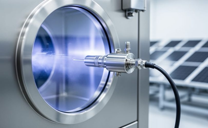
A quartz crystal monitor is a precision measurement instrument that uses the frequency shift of a piezoelectric quartz crystal to measure thin-film deposition rates and thickness with nanometer-level accuracy in real time. In multi-crystalline silicon solar cell production, these devices are essential for controlling anti-reflective coatings, metallization layers, and other critical thin films that directly determine panel efficiency and longevity.
Understanding PV module basics provides the foundation, but achieving the performance specifications stamped on every module requires extraordinary manufacturing precision. A coating just 10 nanometers too thick can reduce light transmission. Too thin, and the silicon beneath oxidizes prematurely. Quartz crystal monitors bridge the gap between theoretical cell design and actual production outcomes by providing the measurement accuracy modern PV manufacturing demands.
This technology operates on a straightforward principle: as material deposits onto the crystal surface during vacuum coating processes, its mass increases and its resonant frequency drops proportionally. That frequency change translates directly into precise thickness measurements. For photovoltaic engineers, this means immediate feedback during silicon nitride deposition, transparent conductive oxide application, and electrode patterning.
This article explains how quartz crystal monitors function within the PV production environment, examines their core components and operational variations, and details their specific applications in multi-crystalline module manufacturing. Whether you’re a manufacturing technician optimizing deposition parameters or an aspiring professional building foundational knowledge, you’ll find practical insights into how precision measurement enables both quality control and process innovation in solar technology.
What a Quartz Crystal Monitor Means in Solar Manufacturing
A quartz crystal monitor is a precision measurement instrument that leverages the piezoelectric properties of quartz to track thin-film deposition in real time during solar cell manufacturing. When technicians deposit anti-reflective coatings, passivation layers, or contact metals onto multi-crystalline silicon wafers, the QCM continuously measures how much material lands on the surface and at what rate, providing immediate feedback that keeps coating thickness within tight tolerances.
The technology works because quartz crystals vibrate at a specific frequency when electrical voltage passes through them. As atoms from the coating process settle onto the crystal surface, the added mass slows the vibration, shifting the resonance frequency in a predictable way. Modern QCM used for thin-film deposition systems convert these frequency changes into nanometer-scale thickness readings, allowing operators to halt deposition the moment a layer reaches its target specification.
- Piezoelectric effect
- The property of quartz and certain other crystals to generate electrical charge under mechanical stress, or conversely, to vibrate when voltage is applied.
- Deposition rate
- The speed at which coating material accumulates on a substrate surface, typically measured in nanometers or angstroms per second during PV manufacturing.
- Resonance frequency
- The natural vibration frequency of a quartz crystal, which decreases as deposited material adds mass to the crystal surface.
- Mass sensitivity
- The QCM’s ability to detect minuscule mass changes on the crystal surface, often in the nanogram range, enabling precise control of ultra-thin coatings.
- Thin-film coating
- A layer of material only a few nanometers to several micrometers thick, applied to solar cells to enhance light absorption, reduce recombination, or form electrical contacts.
This real-time monitoring capability directly supports multi-crystalline module innovation by ensuring each deposited layer meets exact specifications. Without QCMs, manufacturers would rely on post-process inspection, discovering thickness errors only after wasting time, materials, and energy on defective cells.
How Quartz Crystal Monitoring Works
The Piezoelectric Measurement Principle
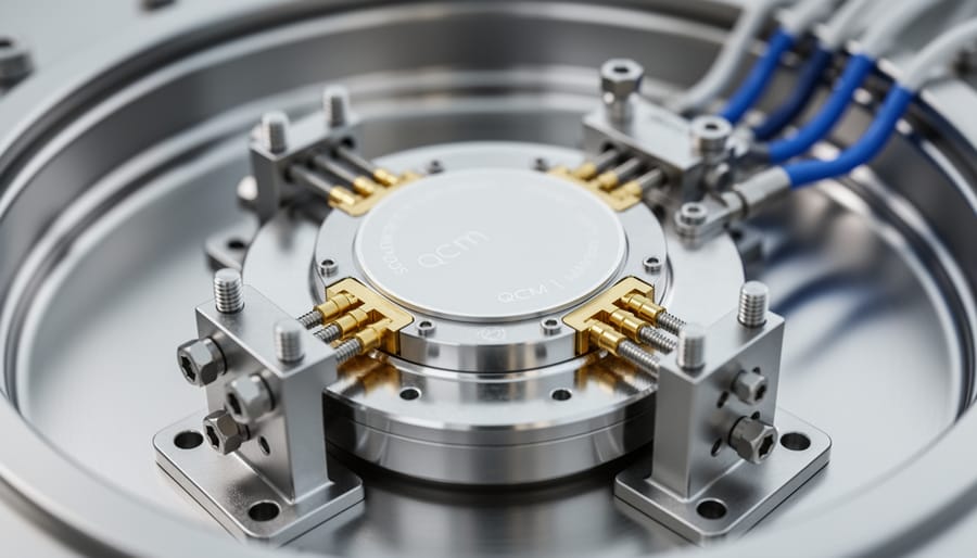
Quartz crystals exhibit a fundamental property called piezoelectricity, when you apply an alternating electrical voltage across the crystal’s surface, it vibrates at a precise resonant frequency determined by its physical dimensions, cut angle, and material properties. A standard 6 MHz crystal oscillates exactly six million times per second under ideal conditions, functioning as an extraordinarily stable frequency reference. This predictable behavior makes quartz ideal for measurement applications where consistency matters more than almost any other factor.
When thin-film material deposits onto the crystal surface during manufacturing processes, it adds mass to the oscillating system. Even nanogram-scale accumulation affects the crystal’s mechanical behavior. The added weight increases the inertia the crystal must overcome with each vibration cycle, causing the resonant frequency to decrease in direct proportion to the deposited mass. This QCM mass causes frequency shift relationship remains linear within practical deposition ranges, typically allowing detection of mass changes as small as a few nanograms per square centimeter, equivalent to fractions of an atomic layer.
The frequency change occurs immediately as material lands on the crystal, enabling real-time tracking of deposition progress. A 1 Hz frequency drop might represent 0.1 nanometers of silicon nitride accumulation, depending on the crystal’s sensitivity and the material’s density. Monitoring equipment continuously measures this frequency shift throughout the coating process, providing operators with instantaneous feedback on deposition rate and accumulated thickness without interrupting production or damaging the substrate.
From Frequency Shift to Thickness Calculation
The monitoring system translates raw frequency shifts into actionable deposition data through mathematical relationships established in the 1950s. At the heart of this conversion lies the Sauerbrey equation relates mass changes to frequency changes with remarkable precision. This formula establishes that frequency decrease is directly proportional to the mass deposited per unit area on the crystal surface.
The equation requires input of material-specific parameters, density and acoustic impedance, to accurately convert from mass to physical thickness. For silicon nitride anti-reflective coatings, manufacturers program different density values than for aluminum oxide passivation layers, ensuring each material yields correct thickness readings despite different atomic structures. This specificity matters because a 100 Hz frequency shift means different physical thicknesses depending on whether you’re depositing silver contacts or titanium dioxide.
Modern controllers perform these calculations continuously, displaying deposition rate in angstroms per second and accumulated thickness in nanometers. The system updates multiple times per second, allowing operators to adjust process parameters mid-run if deposition rates drift from target specifications. Temperature compensation algorithms refine the calculations further, accounting for thermal expansion of the crystal itself during elevated-temperature processes common in multi-crystalline module fabrication.
Components and Variants of Quartz Crystal Monitoring Systems
Single vs. Multi-Channel Systems
Single-channel quartz crystal monitors serve R&D labs and pilot-scale coating trials where engineers need to validate deposition parameters at a single reference point. These basic systems measure film growth on one sensor positioned strategically in the vacuum chamber, providing real-time thickness data sufficient for process development and small-batch experiments.
Multi-channel systems transform this capability into production-scale quality assurance by monitoring deposition uniformity across multiple zones simultaneously. In multi-crystalline module manufacturing, where substrate dimensions can exceed one meter, tracking film thickness at four, six, or even twelve sensor locations reveals spatial variations that single-point monitoring misses entirely. A coating process might deposit 80 nanometers at chamber center but only 72 nanometers at the edges, creating efficiency losses across finished panels. Multi-channel QCMs detect these gradients in real time, enabling immediate adjustments to source geometry, substrate rotation, or process pressure.
The choice between configurations mirrors the debate around multi-crystalline vs monocrystalline production philosophies: balancing precision requirements against manufacturing throughput and cost constraints. High-volume facilities typically deploy multi-channel systems on critical coating steps while reserving single-channel monitors for less sensitive processes.
Water-Cooled and High-Temperature Variants
Manufacturing environments for multi-crystalline solar modules often subject quartz crystal sensors to extreme thermal conditions that would compromise standard room-temperature designs. Water-cooled sensor heads address this challenge by circulating coolant through integrated channels that maintain the crystal at stable operating temperatures even when positioned near high-temperature deposition sources or substrates heated above 300°C. This cooling prevents thermal drift in frequency readings and extends crystal lifespan in demanding processes like PECVD silicon nitride deposition.
High-temperature variants incorporate thermally resistant quartz cuts (AT-cut crystals) and specialized mounting assemblies that tolerate elevated chamber temperatures while preserving measurement accuracy. Some designs combine active cooling with thermal shielding to protect electronics while allowing the sensor face to approach substrate temperatures for representative thickness measurements. Process engineers select configurations based on deposition method, substrate temperature, and required proximity to the coating zone, critical decisions that directly impact measurement reliability during anti-reflective coating and passivation layer formation.
Applications in Multi-Crystalline Module Manufacturing
Anti-Reflective Coating Optimization
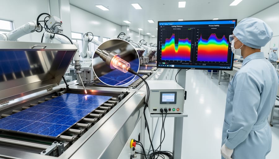
Anti-reflective coatings transform how photons interact with multi-crystalline silicon cells. A silicon nitride layer deposited at precisely 75-80 nanometers can reduce surface reflection from roughly 30% down to under 5%, dramatically increasing the photons available for conversion. Even a 5-nanometer deviation from the optimal thickness shifts the destructive interference wavelength, allowing more blue or red light to reflect away instead of entering the cell. This precision matters because each percentage point of additional reflection translates directly to lost power output across thousands of modules.
Quartz crystal monitors enable real-time thickness control during plasma-enhanced chemical vapor deposition of these coatings. As silicon nitride accumulates on the sensor crystal, the frequency shift allows operators to stop deposition within 2-3 nanometers of the target thickness. This capability proves essential for multi-crystalline substrates, where surface texture variations already challenge uniformity. Without QCM feedback, manufacturers must rely on timed deposition runs calibrated periodically, risking batch-to-batch variation that compounds into efficiency losses. The monitor essentially closes the control loop, letting each coating reach its optical ideal regardless of minor chamber condition changes or feedstock variations.
Passivation Layer Quality Control
Surface passivation layers are critical in multi-crystalline silicon cells, where grain boundaries and crystal defects create numerous recombination sites that reduce conversion efficiency. Quartz crystal monitors provide real-time verification that passivation materials, primarily aluminum oxide (Al₂O₃), silicon oxide (SiO₂), and silicon nitride with varying compositions, deposit at the precise thicknesses required to minimize carrier losses.
In multi-crystalline cells, even a 2-3 nanometer deviation in passivation layer thickness can measurably affect surface recombination velocity. QCMs detect frequency shifts corresponding to sub-nanometer deposition increments, enabling process engineers to maintain consistent passivation quality across production batches. This precision is particularly important for aluminum oxide layers, which typically range from 5 to 30 nanometers and provide both chemical passivation through negative fixed charges and field-effect passivation that repels minority carriers from defect-rich surfaces.
For silicon oxide passivation applied via atomic layer deposition or plasma-enhanced chemical vapor deposition, quartz crystal monitoring ensures uniform coverage across the textured surfaces characteristic of multi-crystalline wafers. Process control at this level directly translates to higher open-circuit voltages and improved fill factors in finished modules.
Metallization and Contact Formation
During metallization, quartz crystal monitors track the deposition of aluminum back-surface fields and silver front contacts with nanometer precision. These metal layers collect and transport photogenerated current, making their thickness and uniformity direct determinants of series resistance and fill factor in finished modules.
Aluminum deposition typically occurs via thermal evaporation or sputtering, with QCMs verifying that the back contact achieves 1-3 micrometers thickness across the entire wafer surface. Insufficient aluminum coverage creates high-resistance areas that throttle current flow. Excessive deposition wastes expensive materials and increases production costs without performance gains.
Silver contact formation demands even tighter tolerances. Front-grid fingers measuring 50-100 micrometers wide require uniform height to balance conductivity against optical shading. QCMs enable process engineers to hold silver deposition rates within 2-5% variation, ensuring consistent contact resistance across production batches.
Multi-channel monitoring systems positioned at different substrate locations detect uniformity issues before they compromise yield. When deposition rate diverges between monitoring points, operators adjust source positioning or chamber parameters immediately rather than scrapping finished cells during electrical testing.
Advantages Over Alternative Monitoring Methods
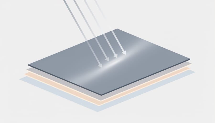
Quartz crystal monitors deliver distinct advantages over alternative measurement techniques used in thin-film deposition processes. While optical methods like ellipsometry and reflectometry can measure film thickness with excellent accuracy, they require transparent substrates and involve complex mathematical models to interpret reflected light data. QCMs operate independently of substrate optical properties, making them versatile across diverse material combinations common in multi-crystalline module production.
The real-time feedback capability of quartz crystal monitoring stands out as its primary production advantage. Unlike stylus profilometry or atomic force microscopy, which measure thickness only after deposition completes, QCMs provide continuous thickness and rate data during the coating process. This immediate feedback enables operators to adjust deposition parameters on the fly, preventing costly batch failures and supporting sustainable manufacturing practices by reducing material waste.
QCMs are fundamentally non-destructive, requiring no sample preparation or post-process handling that could damage delicate coatings. Stylus profilometry involves physical contact that can scratch soft films, while cross-sectional scanning electron microscopy requires destructive sample cutting. The quartz sensor sits inside the deposition chamber without touching the actual substrate being coated, monitoring the process environment rather than the product itself.
Nanometer-level precision distinguishes quartz crystal monitors from thickness estimation methods based on deposition time or power settings. Modern QCM systems resolve mass changes equivalent to sub-nanometer film thickness, far exceeding the accuracy of process-parameter-based calculations. This precision proves essential for manufacturing passivation and anti-reflective layers where thickness variations of just a few nanometers significantly affect optical and electrical performance.
The combination of real-time response, non-destructive operation, and nanometer resolution makes QCMs the preferred choice for high-volume photovoltaic production lines where process control directly determines manufacturing yield and module efficiency outcomes.
Calibration and Accuracy Considerations
Maintaining measurement precision in multi-crystalline production environments requires systematic attention to calibration protocols and accuracy-influencing variables. Even the most sophisticated quartz crystal monitoring systems drift from specification without proper maintenance, potentially compromising the tight tolerances that separate breakthrough efficiency gains from marginal improvements.
The tooling factor represents the most critical calibration parameter in production QCM systems. This dimensionless number accounts for the geometric relationship between where material deposits on the monitoring crystal versus where it deposits on actual substrates, compensating for differences in deposition angles, crystal shielding, and chamber positioning. Determining accurate tooling factors demands depositing calibrated films under production conditions, measuring actual thickness with independent methods like ellipsometry or X-ray fluorescence, then adjusting the QCM reading to match reality. Multi-crystalline facilities typically establish unique tooling factors for each coating material and chamber configuration, updating these values quarterly or whenever process parameters change.
Crystal replacement schedules directly affect long-term measurement reliability. Quartz sensors accumulate stress fractures and mass loading over repeated deposition cycles, gradually degrading their frequency stability and sensitivity. Most production environments replace crystals after specific mass thresholds rather than fixed time intervals, commonly when accumulated film thickness reaches 10-20 micrometers, though this varies by material density and deposition rates.
Environmental compensation addresses temperature fluctuations that alter quartz resonance independently of deposited mass. Production-grade controllers incorporate temperature sensors and correction algorithms, but maintaining stable thermal conditions around sensor heads eliminates a major error source. Effective practices include:
- Verifying calibration against reference standards every 30-90 days
- Maintaining material-specific tooling factors for each coating process
- Implementing automatic temperature compensation in controller settings
- Tracking crystal service life and replacing before sensitivity degrades
Documentation of calibration history enables trend analysis that catches gradual drift before it impacts product quality. The most innovative multi-crystalline manufacturers treat QCM calibration as integral to process control rather than periodic compliance activity, recognizing that nanometer-scale thickness variations translate directly to efficiency differences in finished modules.
Educational Pathways for Understanding Process Monitoring
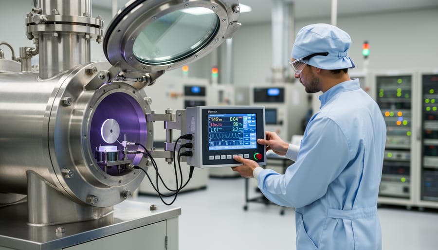
Understanding quartz crystal monitoring technology requires a foundation in materials science, process engineering, and quality control principles. Aspiring photovoltaic professionals can build this expertise through several educational pathways that bridge academic theory with manufacturing realities.
University programs in materials engineering, semiconductor physics, and renewable energy technology now regularly incorporate thin-film deposition and process monitoring into their curricula. Courses in vacuum technology, surface science, and metrology provide the theoretical grounding needed to understand how piezoelectric sensors translate physical phenomena into actionable production data. Laboratory components often include hands-on experience with deposition equipment and measurement instruments similar to those used in commercial PV manufacturing.
Mose Solar collaborates with academic institutions to ensure educational content reflects current industry practices. These partnerships help students connect classroom concepts, frequency response, mass loading, calibration protocols, to real-world challenges like maintaining coating uniformity across large substrates or troubleshooting sensor drift during production runs.
Online educational programs offer flexible learning for working professionals transitioning into advanced manufacturing roles. Specialized modules covering quality assurance in PV production typically address statistical process control, measurement uncertainty, and the integration of monitoring systems into automated production lines. Self-paced coursework allows technicians and engineers to develop expertise in process monitoring while maintaining their current positions.
Short-term certification programs and vendor training sessions provide targeted instruction on specific monitoring platforms, covering equipment operation, data interpretation, and preventive maintenance procedures essential for production environments.
Common Questions About Quartz Crystal Monitors in PV Production
What level of measurement precision can quartz crystal monitors achieve in production environments?
Modern QCM systems routinely measure film thickness with sub-nanometer resolution, typically achieving precision within 0.1-0.5 nanometers under controlled conditions. Actual production precision depends on proper calibration, thermal stability, and regular crystal replacement schedules.
How long do quartz crystals last before requiring replacement?
Crystal lifespan varies with deposition rate and material properties, but typically ranges from several hours to several days of continuous operation. When accumulated film thickness creates excessive frequency shift or damping, crystals must be replaced to maintain accuracy.
Are quartz crystal monitors compatible with all thin-film deposition methods used in solar manufacturing?
QCMs work effectively with physical vapor deposition techniques including thermal evaporation, sputtering, and electron-beam evaporation commonly used for anti-reflective coatings and passivation layers. They are less suited for chemical vapor deposition or plasma-enhanced processes where reactive gases may interfere with crystal oscillation.
What are typical cost considerations when implementing QCM systems in production lines?
Initial investment includes sensor heads, controllers, and integration hardware, with multi-channel systems commanding higher prices for large-area monitoring. Ongoing costs involve crystal replacement, calibration verification, and occasional sensor maintenance, though these expenses are generally modest compared to the quality improvements and yield gains QCMs enable.
These practical questions reflect common concerns among professionals entering advanced PV manufacturing roles. Understanding measurement capabilities helps technicians set realistic expectations for process control. Crystal lifespan directly affects operational planning and consumable budgeting in high-volume production. Compatibility considerations guide equipment selection when designing or upgrading deposition systems for multi-crystalline modules. Integration with automated process control represents another frequent inquiry: modern QCM systems readily interface with programmable logic controllers and supervisory software, enabling closed-loop thickness control where deposition parameters adjust automatically based on real-time measurements. This automation reduces operator burden while maintaining the precision that drives continuous innovation in module efficiency and manufacturing consistency.
Quartz crystal monitoring stands as a foundational technology in the ongoing evolution of multi-crystalline solar modules. As manufacturers push efficiency boundaries and reduce production costs, the nanometer-level precision these instruments provide becomes increasingly critical. Every incremental gain in module performance, whether through optimized anti-reflective coatings, enhanced passivation layers, or precise metallization, relies on the real-time measurement capabilities that QCM systems deliver during thin-film deposition processes.
The relationship between measurement science and solar energy advancement isn’t coincidental. Multi-crystalline technology continues to compete effectively in global markets precisely because manufacturers can control process variables with unprecedented accuracy. Quartz crystal monitors enable this control, transforming what would be trial-and-error processes into repeatable, scalable manufacturing operations that consistently produce higher-efficiency panels.
For aspiring professionals entering the photovoltaic industry, understanding process monitoring technologies like QCMs represents essential knowledge. The measurement principles underlying these instruments connect directly to broader concepts in semiconductor physics, materials science, and quality assurance that define modern solar manufacturing. Universities and specialized educational programs increasingly recognize this connection, integrating process control fundamentals into renewable energy curricula to prepare the next generation of engineers and technicians.
As multi-crystalline module innovation accelerates, the precision measurement tools supporting that progress will only grow more sophisticated. Mastering these technologies positions professionals to contribute meaningfully to an industry where small improvements in process control translate directly into cleaner, more affordable energy worldwide.