The silicon wafer beneath every solar panel tells a story of manufacturing precision that directly determines energy output, production costs, and long-term system performance. Monocrystalline and polycrystalline technologies diverge at the crystallization stage—where molten silicon either forms a single, uniform crystal structure or multiple crystal fragments—creating fundamental differences that cascade through efficiency ratings, temperature coefficients, space requirements, and ultimately, project economics.
Understanding these manufacturing distinctions empowers photovoltaic professionals to make informed specification decisions based on site constraints, budget parameters, and performance expectations rather than marketing claims alone. The Czochralski process produces monocrystalline ingots with uniform atomic alignment, achieving 17-22% conversion efficiency but requiring higher energy inputs and material waste. Conversely, directional solidification creates polycrystalline blocks with visible grain boundaries, delivering 15-17% efficiency at significantly reduced production costs.
This production-focused comparison examines how crystal formation methods influence cell architecture, manufacturing scalability, material utilization, and environmental footprints—equipping aspiring professionals with the technical foundation necessary for contributing to increasingly sophisticated solar deployment strategies in residential, commercial, and utility-scale applications.
The Crystal Growth Foundation: Where Mono and Poly Diverge

The Czochralski Process: Creating Perfect Silicon Crystals
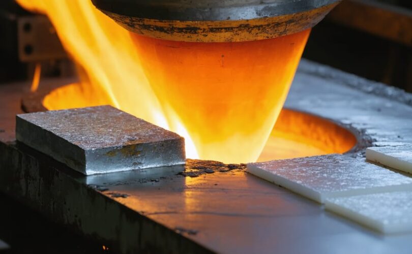
The Czochralski process represents the cornerstone of monocrystalline silicon production, demanding precision engineering and substantial time investment. This method creates the exceptionally pure, uniform crystal structure that distinguishes monocrystalline panels from their polycrystalline counterparts.
The process begins with high-purity polysilicon chunks melted in a quartz crucible at approximately 1,414°C—just above silicon’s melting point. Temperature control remains critical throughout, with variations of even a few degrees potentially compromising crystal quality. Manufacturers maintain an inert atmosphere, typically argon gas, to prevent contamination during the delicate pulling operation.
A seed crystal—a small rod of perfectly oriented single-crystal silicon—is carefully lowered to touch the molten surface. As the seed makes contact, operators slowly rotate and withdraw it at precisely controlled rates, typically 1-2 millimeters per minute. The molten silicon adheres to the seed crystal and solidifies in its exact crystallographic orientation, gradually forming a cylindrical ingot.
This continuous pulling process, spanning 24-36 hours for a single ingot, requires constant monitoring of diameter, temperature gradients, and rotation speed. The resulting monocrystalline ingot typically measures 200-300mm in diameter and up to two meters in length, weighing several hundred kilograms.
The Czochralski method’s extended timeframe and stringent requirements significantly increase production costs compared to polycrystalline casting. However, this investment yields silicon with uniform atomic structure and minimal crystal defects—fundamental characteristics that enable monocrystalline panels’ superior efficiency performance in photovoltaic applications.
Directional Solidification: The Faster Polycrystalline Route
Polycrystalline silicon ingots employ directional solidification, a fundamentally different casting approach that prioritizes manufacturing efficiency. Molten silicon is poured directly into square molds and allowed to cool gradually from bottom to top. This process creates multiple crystal structures as the silicon solidifies, with grains forming boundaries where different crystals meet.
The directional solidification method offers significant manufacturing advantages. Production cycles complete in approximately 20-30 hours compared to days required for monocrystalline growth, substantially reducing energy consumption and equipment utilization costs. The square ingot shape also eliminates material waste during cell cutting, as no edges need trimming to achieve uniform dimensions.
However, these efficiencies introduce performance trade-offs. The multiple crystal boundaries within polycrystalline material create resistance pathways that impede electron flow, reducing overall conversion efficiency. Grain boundaries act as recombination sites where charge carriers can be lost before contributing to electrical current. This fundamental structural difference explains the typical 15-17% efficiency range for polycrystalline panels compared to 18-22% for monocrystalline variants.
Despite lower efficiency, the cost-effectiveness of directional solidification made polycrystalline technology dominant during solar energy’s rapid expansion phase, particularly for large-scale installations where available space offset efficiency limitations.
Production Efficiency and Material Utilization
Silicon Purity Requirements and Waste Generation
Silicon purity requirements fundamentally distinguish these manufacturing approaches, directly impacting production efficiency and waste generation. Monocrystalline production demands exceptionally high-purity silicon—typically 99.9999% pure (6N grade)—to enable single-crystal formation through the Czochralski or float-zone processes. This stringent requirement necessitates additional purification steps, increasing energy consumption by approximately 15-20% compared to polycrystalline production.
Polycrystalline manufacturing tolerates slightly lower purity levels—generally 99.999% (5N grade)—because the casting process accommodates multiple crystal boundaries. This reduced purity threshold translates to fewer processing stages and lower initial material costs, though the performance differential reflects this compromise.
Waste generation patterns reveal nuanced efficiency considerations. Traditional monocrystalline wafer production generated substantial kerf loss—silicon waste from cutting cylindrical ingots into pseudo-square wafers—historically reaching 40-50% material loss. However, diamond wire sawing technology has revolutionized this metric, reducing kerf loss to approximately 10-15% while enabling thinner wafer production. This advancement significantly improves monocrystalline material efficiency.
Polycrystalline production inherently generates less structural waste because rectangular ingots maximize wafer yield without corner trimming. Material utilization typically reaches 85-90%, though the casting process itself may produce more silicon fines and off-spec material requiring reprocessing.
Both technologies now incorporate closed-loop recycling systems, recovering silicon dust and rejected wafers for remelt applications. These initiatives have improved overall material efficiency metrics across the photovoltaic industry, with contemporary facilities achieving silicon recovery rates exceeding 95%, benefiting sustainability goals while reducing raw material dependency.
Energy Intensity and Production Time
The manufacturing of monocrystalline and polycrystalline solar panels demonstrates significant variations in energy consumption and production timelines, directly impacting both manufacturing costs and environmental footprints.
Monocrystalline production requires substantially higher energy inputs, consuming approximately 200-250 kWh per kilogram of silicon during the Czochralski crystal growth process. This energy-intensive method involves maintaining temperatures exceeding 1,400°C for extended periods—typically 48-72 hours—to produce a single ingot. The subsequent wire sawing and wafer processing add another 20-30% to the total energy budget. In contrast, polycrystalline manufacturing consumes roughly 30-40% less energy, utilizing 130-170 kWh per kilogram through its casting method, which requires only 12-24 hours for ingot formation.
Production cycle times reflect these energy differences. A complete monocrystalline manufacturing cycle from raw silicon to finished wafer spans approximately 5-7 days, whereas polycrystalline production completes within 3-4 days. This temporal advantage translates to higher throughput rates for polycrystalline facilities, with modern plants achieving 15-20% greater output capacity using comparable equipment.
However, these efficiency metrics must be contextualized against yield rates. Monocrystalline processes typically achieve 95-98% usable wafer yields due to superior crystal uniformity, while polycrystalline yields range from 88-92%. Material waste from edge trimming and sawing kerf loss affects both technologies, though monocrystalline’s cylindrical ingots generate approximately 30% more silicon waste during squaring operations. These production characteristics fundamentally influence the economic and environmental calculus that manufacturers and industry stakeholders must consider when selecting manufacturing approaches.
Wafer Processing: From Ingot to Cell
Wire Sawing and Wafer Yield Considerations
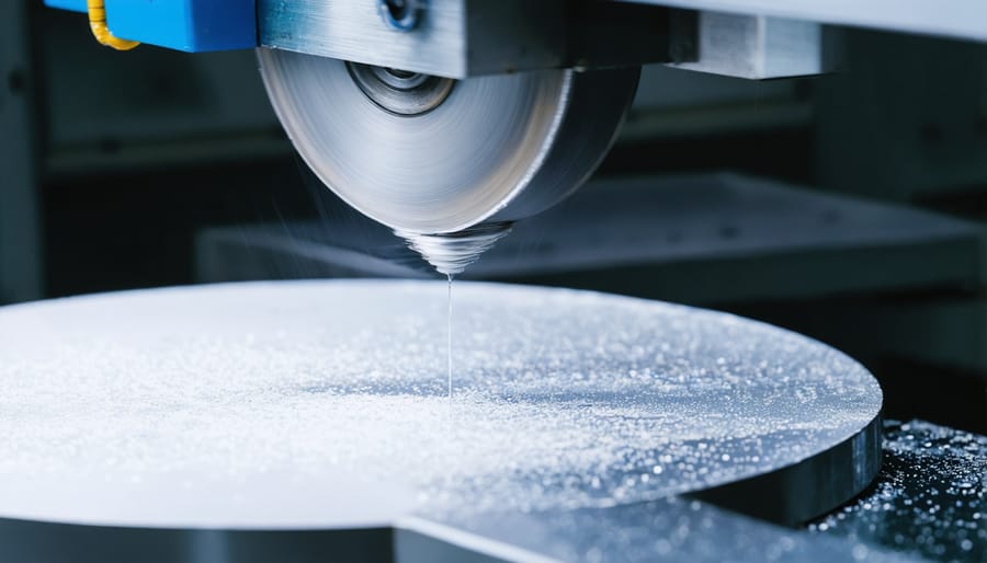
Wire sawing represents a critical juncture where crystalline differences significantly impact manufacturing efficiency and material losses. During this phase of the solar cell manufacturing process, diamond wire saws slice ingots into thin wafers, typically 160-180 micrometers thick.
Monocrystalline ingots present distinct challenges due to their cylindrical shape and uniform crystal structure. The round profile necessitates edge trimming to create pseudo-square wafers, resulting in 10-15% material waste. However, the homogeneous crystal orientation enables predictable cutting behavior and lower breakage rates, typically maintaining wafer yields above 95%.
Polycrystalline ingots, cast into rectangular blocks, eliminate shape-related waste, maximizing material utilization. Yet their multi-directional grain boundaries create inconsistent mechanical stress distribution during sawing. This crystallographic variability increases susceptibility to micro-cracks and wafer breakage, particularly at grain boundary interfaces. Breakage rates can reach 5-8% under suboptimal conditions, though advanced wire tension control and cutting speed optimization have substantially improved yields.
Crystal uniformity ultimately determines sawing precision, with monocrystalline’s structural consistency offsetting its geometric disadvantages in many high-volume manufacturing environments.
Surface Texturing and Light Absorption
The uniform crystal structure of monocrystalline silicon enables manufacturers to apply sophisticated surface texturing techniques that significantly enhance light absorption. During production, chemical etching creates microscopic pyramidal structures aligned along the crystal planes—typically arranged in regular patterns measuring 2-10 micrometers. These pyramids function as light traps, redirecting incident photons that would otherwise reflect away, allowing multiple opportunities for absorption within the silicon lattice.
Polycrystalline wafers present a fundamentally different challenge. The random orientation of crystal grains and the presence of grain boundaries disrupt uniform texturing. When etching solutions encounter these boundaries, they create irregular surface features rather than aligned pyramids. This inconsistency reduces the effectiveness of light-trapping mechanisms, resulting in higher reflectance losses—typically 3-5% more than monocrystalline counterparts even after anti-reflective coating application.
The superior texturing capability of monocrystalline cells directly translates to improved quantum efficiency, particularly in the blue wavelength spectrum where reflectance losses are most pronounced. This manufacturing advantage contributes approximately 0.5-1% to the overall efficiency differential between the two technologies, representing a measurable performance benefit that compounds with other structural advantages throughout the cell’s operational lifetime.
Performance Outcomes: How Production Shapes Efficiency

Efficiency Gains from Uniform Crystal Structure
The superior performance of monocrystalline panels stems directly from their uniform crystal lattice structure, which fundamentally transforms how electrons move through the material. In single-crystal silicon, electrons encounter minimal resistance as they travel through the perfectly aligned atomic structure, achieving electron mobility rates of 1,400 cm²/V·s compared to approximately 1,000 cm²/V·s in polycrystalline silicon.
This structural uniformity translates into measurable efficiency differences. Monocrystalline panels typically achieve conversion efficiencies between 17-22%, while polycrystalline variants reach 15-17%. The performance gap originates from two critical factors: enhanced electron mobility and reduced recombination losses.
Polycrystalline silicon contains grain boundaries—interfaces where different crystal orientations meet. These boundaries act as trap sites where electrons recombine with holes before contributing to electrical current, effectively losing energy as heat rather than generating usable electricity. Research indicates that grain boundary recombination can reduce overall cell efficiency by 2-4 percentage points.
The monocrystalline efficiency advantages become particularly evident under real-world conditions. Single-crystal structures maintain more consistent performance across varying light intensities and temperatures because their homogeneous composition provides predictable electron pathway behavior throughout the material.
Laboratory measurements using electron beam-induced current (EBIC) microscopy demonstrate that carrier lifetimes in monocrystalline silicon exceed 100 microseconds, compared to 20-50 microseconds in polycrystalline materials, directly correlating with improved charge collection efficiency and higher power output per unit area.
Long-Term Degradation and Production Quality
The manufacturing precision inherent to monocrystalline production directly correlates with superior long-term stability. Monocrystalline panels typically exhibit degradation rates of 0.3-0.5% annually, while polycrystalline modules degrade at 0.5-0.8% per year. This difference stems primarily from defect density variations between the two production methods.
The Czochralski process used for monocrystalline wafers creates uniform crystal structures with minimal grain boundaries, resulting in fewer electron-hole recombination sites. Polycrystalline ingots, conversely, contain numerous grain boundaries where crystallographic imperfections accumulate, accelerating performance decline over decades.
Micro-crack susceptibility represents another critical degradation pathway. Monocrystalline wafers, despite their single-crystal structure, can be more brittle due to uniform cleavage planes. However, modern manufacturing incorporating diamond wire sawing has significantly reduced mechanical stress during wafer production. Polycrystalline panels demonstrate greater mechanical flexibility but suffer from crack propagation along grain boundaries during thermal cycling.
Industry research from leading photovoltaic laboratories indicates that after 25 years, monocrystalline panels typically retain 90-92% of original capacity, compared to 85-88% for polycrystalline equivalents. These degradation profiles directly influence long-term energy yield calculations and project financing models, making production quality assessment essential for professional system designers evaluating lifetime performance guarantees.
Economic and Environmental Implications for the Industry
Production Cost Breakdown and Market Pricing
The price premium of monocrystalline panels—typically 10-20% higher than polycrystalline alternatives—stems directly from their manufacturing complexity. The Czochralski process required to grow single-crystal silicon ingots demands significantly more energy and time compared to the casting method used for polycrystalline production. Single-crystal growth operates at precise temperatures around 1,414°C for extended periods, consuming approximately 30-40% more energy per kilogram of silicon produced.
Additional cost factors include higher material waste during the wafering process. Monocrystalline ingots are cylindrical, requiring corner trimming to create pseudo-square cells that fit standard panel dimensions. This geometric inefficiency results in 12-15% silicon waste, compared to 8-10% for cast polycrystalline blocks that naturally form rectangular shapes.
However, economies of scale are progressively narrowing this pricing gap. Global production expansion, particularly in Asian manufacturing hubs, has driven down per-watt costs for both technologies. Between 2010 and 2023, monocrystalline module prices decreased by approximately 90%, with production efficiencies improving yield rates and reducing waste. Advanced diamond wire sawing techniques have also minimized kerf loss—the material removed during wafer cutting—from 180 micrometers to under 100 micrometers.
Market dynamics further influence pricing differentials. As monocrystalline technology achieves higher conversion efficiencies (now exceeding 22% for commercial modules), the cost-per-watt gap continues closing despite absolute price differences. For large-scale installations where space optimization matters, the superior power density of monocrystalline panels often justifies their premium, fundamentally altering traditional cost-benefit calculations in professional procurement decisions.
Carbon Footprint and Sustainability Considerations
Both monocrystalline and polycrystalline panel production carry significant environmental considerations, though their impacts differ in important ways. Monocrystalline manufacturing requires higher energy inputs due to the Czochralski process, which demands precise temperature control and longer processing times. This translates to greater embodied energy—typically 15-20% more than polycrystalline production. However, monocrystalline panels often achieve shorter energy payback periods (1.5-2 years) compared to polycrystalline variants (2-2.5 years) because their superior efficiency generates more electricity over their operational lifetime.
The environmental footprint of production extends beyond energy consumption to include silicon waste generation. Polycrystalline manufacturing utilizes silicon more efficiently, minimizing raw material waste during casting. Conversely, monocrystalline production generates approximately 30-40% silicon waste during ingot shaping and wire sawing.
From a lifecycle perspective, both technologies demonstrate positive environmental returns, offsetting their production impacts within 2-3 years while operating efficiently for 25-30 years. Modern manufacturing facilities increasingly employ renewable energy sources and closed-loop recycling systems, progressively reducing the carbon intensity of both panel types.
Emerging Production Technologies: PERC and Beyond
Advanced manufacturing innovations are reshaping the competitive landscape between monocrystalline and polycrystalline technologies, with PERC technology emerging as a pivotal development. PERC, or Passivated Emitter and Rear Cell technology, adds a dielectric passivation layer to the rear surface of solar cells, significantly reducing electron recombination and enhancing light capture through rear-side reflection.
While PERC can theoretically be applied to both cell types, monocrystalline substrates derive substantially greater benefits from this enhancement. The superior crystalline structure of monocrystalline silicon allows PERC modifications to achieve efficiency gains of 1-2 percentage points more effectively than polycrystalline applications. This efficiency advantage, combined with declining production costs, has accelerated monocrystalline PERC adoption across commercial and utility-scale installations.
Current manufacturing data indicates that PERC-enhanced monocrystalline cells routinely achieve efficiencies exceeding 22%, with research prototypes reaching 24-26%. Polycrystalline PERC variants, constrained by grain boundary limitations, typically plateau around 19-20% efficiency. This widening performance gap has profound implications for technology selection in production planning.
Beyond PERC, emerging technologies such as TOPCon (Tunnel Oxide Passivated Contact), HJT (Heterojunction Technology), and bifacial cell designs predominantly favor monocrystalline substrates. These next-generation approaches require the crystalline uniformity that only Czochralski-grown ingots provide, further marginalizing polycrystalline production in high-performance applications.
For industry professionals and academic researchers, understanding these technological trajectories is essential for strategic planning. The production landscape increasingly favors monocrystalline manufacturing lines capable of integrating advanced passivation techniques, while polycrystalline facilities face adaptation challenges or potential obsolescence in premium market segments.
Understanding the production differences between monocrystalline and polycrystalline panels forms the foundation for informed decision-making in photovoltaic system design. The manufacturing distinctions—from the Czochralski process creating single-crystal ingots to the directional solidification forming polycrystalline structures—directly influence efficiency ratings, temperature coefficients, space requirements, and total project costs. For PV professionals, this technical knowledge enables accurate client consultations, appropriate technology selection for specific applications, and realistic performance projections. When choosing between panel types, consider installation constraints, budget parameters, and long-term energy goals alongside manufacturing characteristics. The production pathway ultimately determines not just panel specifications but system longevity and return on investment. Mose Solar offers comprehensive educational resources and technical training programs developed in collaboration with leading universities, equipping professionals with deeper insights into manufacturing processes, quality assessment methodologies, and emerging production innovations that continue shaping the photovoltaic industry’s evolution.