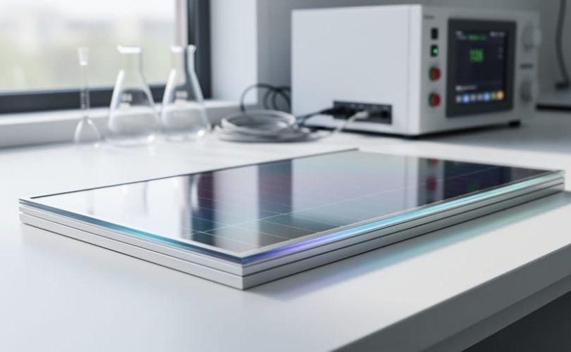
Perovskite solar cells have transitioned from laboratory curiosity to commercial production, with manufacturing facilities now operating across Asia, Europe, and North America. The crystalline material at their core can be deposited through solution-processing techniques that work at temperatures below 150°C, a stark contrast to the energy-intensive methods required for traditional silicon panels. Production methods currently fall into three categories: spin-coating for research applications, slot-die and blade coating for pilot-scale manufacturing, and vapor deposition for specialized applications requiring superior film uniformity.
The production advantage is substantial. Where silicon wafer fabrication requires temperatures exceeding 1,400°C and complex multi-step processes, perovskite layers form through simple chemical reactions involving methylammonium iodide and lead compounds. Several manufacturers reported 2025 production costs below $0.15 per watt, though long-term stability concerns have prevented widespread commercial deployment. The International Energy Agency documented efficiency records reaching 26.1% for single-junction cells and 33.9% for perovskite-silicon tandem configurations.
Commercial viability hinges on resolving degradation under heat, moisture, and UV exposure. Current encapsulation strategies extend operational lifetimes to approximately five years under accelerated testing protocols, well short of the 25-year standard for silicon modules. Through partnerships with institutions including the National Renewable Energy Laboratory and Oxford University, researchers are developing barrier coatings and compositional modifications that address these limitations while maintaining the low-temperature processing advantages that make perovskite production economically compelling.
What Makes Perovskite Different From Traditional Solar Materials
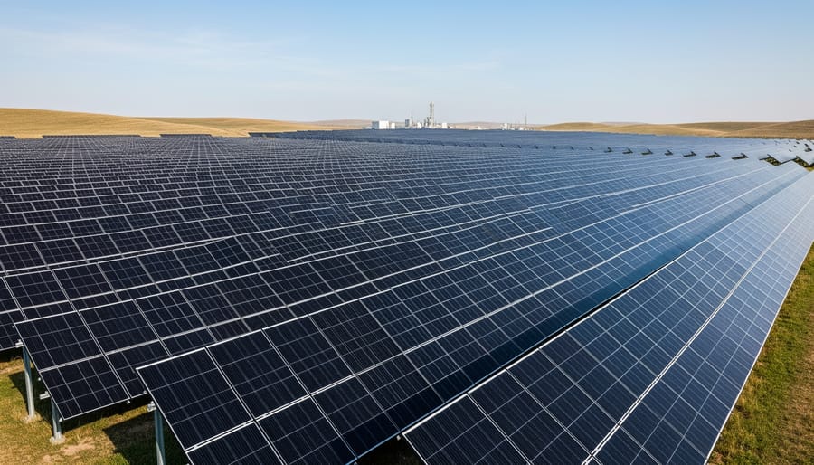
Silicon ruled solar for sixty years because it was reliable and understood, but perovskite’s advantage comes down to physics, not gradual refinement. Where silicon requires high-temperature processing and thick crystalline wafers to capture enough photons, perovskite absorbs light far more efficiently across a broader spectrum while remaining flexible and solution-processable at near room temperature.
- Perovskite Crystal Structure
- An ABX₃ arrangement where organic cations (A), metal cations (B), and halide anions (X) form a three-dimensional lattice. This geometry allows rapid charge carrier movement and tunable light absorption properties.
- Bandgap Tunability
- The energy threshold at which a material absorbs light and generates electricity. Perovskites allow precise adjustment of this threshold by changing halide composition, enabling optimization for different wavelengths or tandem cell architectures.
- Absorption Coefficient
- A measure of how quickly material captures photons. Perovskite’s coefficient reaches 10⁵ cm⁻¹, meaning a layer just 500 nanometers thick absorbs as much light as a 200-micron silicon wafer.
- Direct Bandgap Material
- A semiconductor where electrons transition directly from valence to conduction band without requiring lattice vibrations. This makes perovskite dramatically more efficient at converting absorbed photons to electrical current than indirect bandgap silicon.
Understanding crystal structure basics reveals why this architecture matters. The perovskite lattice permits defect tolerance that silicon cannot match, meaning imperfections that would cripple silicon cell performance barely affect perovskite efficiency. Charge carriers move through perovskite with diffusion lengths exceeding one micron despite solution processing, achieving performance metrics that took silicon decades of refinement to reach.
The practical implications reshape manufacturing economics. A typical silicon cell requires wafers 150-200 microns thick, produced at temperatures exceeding 1,400°C through energy-intensive Czochralski growth. Perovskite layers function at 300-1,000 nanometers, deposited from liquid solutions below 150°C, cutting material use by 99% and energy consumption proportionally. The same physics enabling thin layers makes perovskite naturally flexible, opening applications on curved surfaces, building-integrated installations, and portable devices where rigid silicon never competed.
This represents fundamental material advantage, not incremental efficiency gains. Silicon approaches its theoretical 29% single-junction limit after six decades of optimization. Perovskite already exceeds 26% in certified laboratory cells and pushes theoretical limits past 33% in tandem configurations, all while requiring a fraction of the material, energy, and processing complexity that made silicon the industry standard.
Core Production Techniques Bringing Perovskite to Market
Solution-Based Coating Methods
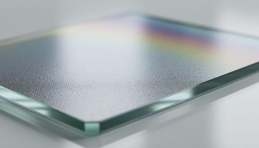
Solution processing stands out as the most accessible entry point for perovskite manufacturing because it works at temperatures below 150°C and uses equipment adapted from existing coating industries. The perovskite precursor dissolves in a solvent to create an ink that spreads across a substrate, then crystallizes as the solvent evaporates. This simplicity masks sophisticated control requirements that separate research-grade films from commercial products.
Spin coating dominates laboratory work for good reason. A substrate spins at 1,000-6,000 RPM while the perovskite solution deposits and spreads by centrifugal force. Researchers achieve exceptional film uniformity across small areas, typically under 2 cm². The technique excels at testing new formulations quickly, but scaling to commercial panel sizes hits physical limits. Larger substrates create edge-thickness variations and waste most of the solution that flies off during spinning.
Blade coating and slot-die coating solve the scalability problem by using a moving blade or pressurized slot to spread solution across stationary or slowly moving substrates. Blade coating, conceptually similar to screen printing, drags a sharp edge across the surface at controlled height and speed. Slot-die systems pump solution through a narrow slot onto a substrate moving underneath, enabling continuous roll-to-roll processing for flexible panels. Both methods achieve 90%+ material utilization compared to spin coating’s 5% and work at production speeds exceeding one meter per minute.
Film quality hinges on crystallization control during drying. Solvent engineering selects combinations that evaporate at rates promoting dense, pinhole-free crystals. The anti-solvent technique improves this further by dripping a non-solvent (like toluene or chlorobenzene) onto the wet film during coating, rapidly extracting the primary solvent and triggering uniform nucleation. This produces the compact, mirror-smooth perovskite layers that deliver 20%+ efficiency rather than the rough, incomplete films that plagued early attempts.
Vapor Deposition Approaches
Vapor deposition methods deliver the precision perovskite manufacturing needs for high-efficiency architectures. Thermal evaporation works by heating source materials in a vacuum chamber until they vaporize and condense onto substrates as uniform thin films. This approach gives manufacturers tight control over layer thickness and composition, critical when building tandem cells where even nanometer-scale variations affect performance. Chemical vapor deposition (CVD) takes a different route, using chemical reactions of gaseous precursors to form perovskite films at the substrate surface. CVD excels at creating highly uniform layers across large areas, making it particularly valuable for industrial-scale tandem production where consistency determines yield rates.
The uniformity advantage matters most in perovskite tandem solar cells, which stack a perovskite layer over silicon to capture different wavelengths. Any thickness variation in the top layer creates efficiency losses across the module. Vapor methods minimize these defects better than solution techniques, though they demand significant equipment investment, vacuum chambers, precision heating systems, and gas handling infrastructure push capital costs higher than solution-based lines.
Scalability presents the real challenge. Thermal evaporation struggles with material waste as only a fraction of vaporized material reaches the substrate. CVD requires careful management of toxic or flammable precursor gases, adding safety complexity and operational costs. These factors explain why most manufacturers exploring vapor deposition focus on premium segments like high efficiency solar panels where precision justifies the expense, while solution methods dominate cost-sensitive applications. As solar cell efficiency improvements push tandem architectures toward mainstream adoption, equipment suppliers are working to reduce vapor deposition costs through automated substrate handling and improved material utilization, but the technique still requires higher manufacturing sophistication than solution processing.
Hybrid and Emerging Fabrication Methods
Inkjet printing, screen printing, and spray coating represent the pragmatic middle ground between laboratory precision and industrial-scale production. These techniques adapt proven methods from electronics manufacturing and coating industries, eliminating the vacuum chambers and complex equipment that make vapor deposition expensive while offering better control than simple blade coating.
Inkjet printing deposits perovskite precursor solutions as controlled droplets, enabling pattern customization and material savings of 40-60% compared to blanket coating methods. Screen printing pushes viscous perovskite pastes through mesh stencils, achieving thicker films suitable for absorber layers in under thirty seconds per panel. Spray coating atomizes solutions into fine mists that deposit uniformly across large substrates, with recent ultrasonic spray systems demonstrating consistent film quality on panels exceeding two square meters.
| Method | Throughput | Film Quality | Best Application |
|---|---|---|---|
| Inkjet Printing | Medium | High precision | Custom designs, R&D |
| Screen Printing | High | Good uniformity | Building-integrated PV |
| Spray Coating | Very high | Scalable quality | Large-format panels |
The real advantage emerges in manufacturing flexibility. A single production line can switch between different perovskite compositions in minutes rather than hours, letting manufacturers respond quickly to market demands for specific efficiency levels or form factors. Startups targeting niche markets like portable solar or architectural integration favor these methods because capital costs run 60-70% lower than establishing vapor deposition facilities, though achieving comparable efficiency still requires careful process optimization and quality control protocols that many are still refining.
Solving the Stability Challenge That Held Perovskite Back
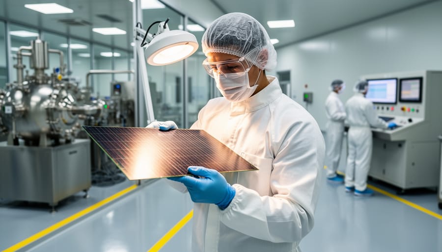
For years, perovskite’s Achilles heel was its fragility. Expose these promising cells to moisture, oxygen, or sustained heat, and their crystalline structure degraded within weeks. That single weakness kept the technology confined to laboratories while silicon dominated commercial production.
The breakthrough came through a three-pronged attack on instability.
Encapsulation technology evolved beyond simple glass sealing. Modern perovskite modules use multi-layer barrier films combining ethylene vinyl acetate with edge sealants that block water vapor transmission to less than 0.0001 grams per square meter per day. Manufacturers now employ laser-edge sealing techniques during production, creating hermetic barriers that prevent moisture ingress at the cell perimeter where degradation typically initiates. These advances mirror broader innovations in PV panel life extension across different solar technologies.
Compositional engineering tackled instability at the molecular level. Pure methylammonium lead iodide (the original perovskite formulation) proved too reactive. Researchers discovered that mixing cations, combining methylammonium with formamidinium, cesium, and rubidium, creates a more stable crystal lattice. The “quadruple cation” formulation developed at Oxford and now widely adopted distributes stress across multiple ionic species, preventing phase transitions that destroy efficiency. Similarly, partial substitution of iodide with bromide or chloride anions strengthens bonds against moisture attack. Production lines adapted by installing precise multi-nozzle deposition systems that blend these components with exact stoichiometry during coating.
Interface stabilization addressed the weak points where perovskite contacts transport layers. Manufacturers introduced self-assembled monolayers between the perovskite film and charge extraction materials, preventing ion migration that causes voltage loss. Passivation treatments using phenethylammonium iodide or other bulky organic molecules seal surface defects where water molecules would otherwise penetrate.
These combined solutions now enable manufacturers to offer 25-year performance warranties matching silicon panels. Accelerated lifetime testing following IEC 61215 standards shows less than 5% degradation after 1,000 hours of damp heat exposure at 85°C and 85% humidity, conditions that would have destroyed first-generation perovskite cells entirely.
Tandem Architecture: Why Perovskite-Silicon Pairs Win
Silicon-based solar cells bump against a hard efficiency ceiling around 29%, a limit imposed by the material’s fixed bandgap. Perovskite breaks through this constraint by stacking on top of silicon in a tandem configuration that splits the solar spectrum between two absorber layers, each optimized for different wavelengths. The perovskite top cell harvests high-energy blue and green photons while allowing red and infrared light to pass through to the silicon layer below. This division of labor pushes combined efficiency beyond 33% in commercial prototypes, with laboratory cells already exceeding 34%.
The key advantage lies in perovskite’s tunable bandgap, adjusted by varying the halide composition during production. Manufacturers typically tune the top cell to around 1.7 electron volts, creating the optimal spectral split with silicon’s 1.1 eV bandgap. This precision matching requires careful control during solution processing or vapor deposition, where slight compositional shifts alter the bandgap and thus the wavelength absorption profile.
Building these multi-junction cells demands more sophisticated production than standalone perovskite panels. The silicon bottom cell often incorporates advanced heterojunction manufacturing for reduced recombination losses, adding process steps before the perovskite layer is applied. Between the two absorbers sits a recombination layer that must allow current to flow without blocking light, typically comprising transparent conductive oxides deposited at temperatures that won’t damage the underlying silicon.
Despite this added complexity, manufacturers pursue tandem architecture because the efficiency gains justify higher production costs. A 33% efficient tandem module generates substantially more power per square meter than a 22% silicon panel, reducing balance-of-system costs like racking, wiring, and installation labor. For utility-scale projects where land and mounting infrastructure represent major expenses, this efficiency premium outweighs the manufacturing challenges, making perovskite-silicon tandems the priority path for commercialization rather than standalone perovskite cells.
Production Scaling and Manufacturing Economics
Perovskite production offers compelling economics compared to traditional silicon manufacturing, though the timeline to market dominance depends heavily on which fabrication method reaches scale first. Raw material costs represent the most dramatic advantage: perovskite precursor materials cost roughly $10-20 per kilogram versus silicon’s polycrystalline production expense of $15-30 per kilogram, but more importantly, perovskite cells use 100-500 times less active material per square meter due to their exceptional light absorption properties. A perovskite layer measuring just 300-500 nanometers thick captures sunlight as effectively as a 180-micron silicon wafer.
Equipment investment varies significantly by technique. Solution-based coating methods like slot-die require modified versions of existing industrial coating lines used in display manufacturing, representing capital costs 40-60% lower than silicon cell fabrication facilities. Thermal evaporation systems demand specialized vacuum chambers running $2-5 million per deposition station, but deliver superior uniformity for tandem architectures where the premium justifies the investment. Screen printing and spray coating occupy the low-cost end, leveraging equipment already proven in organic electronics with minimal adaptation.
Several economic factors are accelerating perovskite’s path to commercial viability:
- Material costs under $0.02 per watt compared to silicon’s $0.05-0.08 per watt at current scales
- Processing temperatures below 150°C versus silicon’s 1400°C, slashing energy consumption by 80-90%
- Deposition speeds reaching 10-30 meters per minute for roll-to-roll methods, triple silicon’s throughput
- Yield rates now exceeding 92% for leading manufacturers using optimized coating protocols
Production speed gives perovskite its clearest competitive edge. Solution processing completes device fabrication in under two hours compared to silicon’s multi-day cycle through numerous high-temperature steps. This throughput advantage compounds at scale, where a gigawatt perovskite line occupies one-third the floor space of equivalent silicon capacity.
Cost parity with silicon modules arrived in pilot production during 2024-2025 for companies using blade coating at 100+ megawatt annual capacity. Industry projections place perovskite at 15-20% cost advantage by 2028 as dedicated gigawatt facilities come online, with tandem perovskite-silicon cells reaching silicon-only pricing despite their added complexity. The economics favor hybrid manufacturing initially, adding perovskite layers to existing silicon infrastructure, before standalone perovskite plants dominate new capacity additions in the 2030s.
Environmental and Safety Considerations in Production
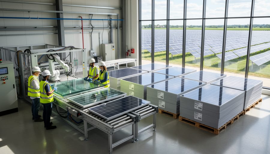
Lead remains the most contentious aspect of perovskite production. The highest-performing formulations contain lead halides, raising legitimate toxicity concerns that manufacturers must address through rigorous containment protocols. Modern production facilities implement closed-loop systems that prevent lead exposure during coating and encapsulation stages. Workers follow strict PPE requirements including respirators and full protective clothing when handling precursor materials. The industry has established monitoring systems that detect airborne lead concentrations at levels 50 times more sensitive than OSHA requirements.
Tin-based perovskites offer a lead-free alternative, but current tin formulations suffer from stability issues and lower efficiency. Research teams at Oxford PV and the National Renewable Energy Laboratory are working to improve tin perovskite performance through compositional engineering, but commercial production remains years away. Until then, the focus stays on preventing lead release through robust encapsulation that isolates the active layer from environmental exposure.
Solvent management presents its own challenges. Solution-based production techniques rely on dimethylformamide (DMF) and dimethyl sulfoxide (DMSO), both requiring proper ventilation and recovery systems. Leading manufacturers now recycle 85-90% of process solvents through distillation, reducing both costs and environmental impact. Waste streams containing trace perovskite materials receive treatment to precipitate heavy metals before disposal, meeting hazardous waste regulations in all major markets.
Lifecycle analysis shows perovskite production consumes 60% less energy than polysilicon manufacturing because it eliminates high-temperature processing. The carbon payback period drops to under six months, compared to 1.5-2 years for conventional silicon panels. End-of-life recycling protocols focus on recovering the transparent conducting oxide layers and glass substrates while safely processing the perovskite layer. As production scales, regulatory frameworks in the EU and US are evolving to establish specific handling standards for perovskite-containing products, ensuring safe integration into the solar industry’s existing infrastructure.
What This Means for Solar Professionals and Industry Stakeholders
The shift toward perovskite production creates immediate demand for professionals who understand both traditional photovoltaic fundamentals and emerging deposition techniques. Engineers with experience in solution processing, thin-film coating, or semiconductor manufacturing find themselves particularly well-positioned, but the field welcomes cross-disciplinary expertise. Process engineers who can optimize coating parameters, quality control specialists familiar with advanced characterization tools, and materials scientists who grasp the chemistry behind film formation all play critical roles in scaling these technologies.
For existing solar professionals, the knowledge gap centers on wet chemistry processes and precise film formation control rather than the electrical theory already mastered. Installation technicians face less disruption since handling and mounting practices remain largely unchanged, though understanding performance characteristics of hybrid perovskite-silicon modules helps with proper system design. Project developers and finance professionals must update their cost models and degradation assumptions as warranty terms and LCOE calculations shift with this new material class.
Mose Solar addresses these training needs through partnerships with universities developing specialized curricula in next-generation photovoltaic manufacturing. These programs combine classroom instruction in perovskite materials science with laboratory access to coating equipment and characterization tools. The educational pathways recognize that career entry points vary, recent engineering graduates, technicians upskilling from silicon production, and researchers transitioning from academia all require different starting points but converge on the same manufacturing competencies that employers now seek.
Perovskite solar panel production has crossed the threshold from laboratory promise to manufacturing reality. The techniques covered here, solution coating, vapor deposition, and emerging hybrid methods, are already being deployed in commercial facilities across the globe. We’re witnessing a technological transition comparable to when crystalline silicon displaced earlier photovoltaic materials, but compressed into a remarkably shorter timeframe.
For solar professionals and aspiring technicians, this isn’t a distant development to monitor casually. The production knowledge base is expanding rapidly, creating immediate demand for workers who understand both traditional PV fundamentals and perovskite-specific manufacturing protocols. Material scientists, process engineers, and quality control specialists familiar with these techniques will find themselves increasingly valuable as production scales through 2026 and beyond.
The stability solutions and tandem architectures discussed here have transformed perovskite from an interesting curiosity into a practical commercial product. Companies are securing warranties, investors are committing capital, and production lines are coming online at an accelerating pace.
Mose Solar collaborates with universities to develop educational programs addressing exactly these emerging manufacturing techniques. Whether you’re entering the solar industry or expanding your existing expertise, staying current with perovskite production innovations positions you at the forefront of photovoltaic technology. Explore our training resources to build the specific skills this industry transformation demands.