3D printing solar panels represents a transformative manufacturing approach that combines additive manufacturing techniques with photovoltaic technology to produce functional solar cells and modules at significantly lower costs than conventional methods. While current 3D-printed panels achieve conversion efficiencies between 3% and 15% (compared to 18-22% for traditional silicon panels), the technology excels in specialized applications where customization, rapid prototyping, and reduced material waste outweigh peak efficiency demands.
The process differs fundamentally from traditional PV cell manufacturing. Instead of slicing silicon wafers and assembling rigid modules, 3D printing deposits photovoltaic materials layer by layer using techniques like inkjet printing, aerosol jet deposition, or direct ink writing. Perovskite and organic photovoltaic materials have emerged as the most compatible semiconductors for this approach, offering solution-based processing that traditional crystalline silicon cannot match.
Economic advantages drive serious industry interest. Capital equipment costs for 3D printing solar cells can run 40-60% lower than conventional production lines, while material utilization approaches 95% compared to 50-60% in traditional wafer-based manufacturing. Production flexibility allows manufacturers to create custom geometries for building-integrated photovoltaics, curved surfaces, and IoT devices without retooling entire production facilities.
The technology faces real limitations. Durability testing shows shorter operational lifespans than conventional panels, typically 10-15 years versus 25-30 years for silicon modules. Efficiency improvements remain incremental rather than revolutionary, with most gains coming from material science advances rather than printing methodology alone.
For professionals evaluating this technology in 2026, the question isn’t whether 3D-printed solar panels will replace traditional manufacturing, but rather where their unique advantages justify deployment despite current performance gaps.
Understanding 3D Printing Technologies in Solar PV Production
Materials Used in 3D Printed Solar Components
The materials palette for 3D printed solar components extends well beyond traditional silicon wafers, opening manufacturing possibilities that conventional processes cannot achieve.
Photovoltaic inks represent the most direct approach to printing active solar materials. These formulations suspend semiconductor nanoparticles, commonly copper indium gallium selenide (CIGS), cadmium telluride, or perovskite compounds, in carrier fluids that allow precise deposition through inkjet or aerosol jet printing. Current formulations achieve particle sizes between 20 and 200 nanometers, with viscosity carefully controlled to prevent nozzle clogging while maintaining layer uniformity.
Conductive polymers like PEDOT:PSS (poly(3,4-ethylenedioxythiophene) polystyrene sulfonate) serve as transparent electrodes and hole transport layers in printed organic photovoltaics. These materials offer conductivity approaching 1000 S/cm while maintaining optical transparency above 80 percent, making them viable alternatives to indium tin oxide in certain applications.
For metal contacts and busbars, silver nanoparticle pastes dominate due to their high conductivity after sintering, though copper-based alternatives are emerging to reduce material costs. These conductive pastes typically require thermal or photonic sintering at temperatures between 150 and 250 degrees Celsius to achieve bulk-like electrical properties.
Substrate materials must withstand processing temperatures while providing mechanical support. Polyethylene terephthalate (PET) and polyimide films work for low-temperature processes, while glass and ceramic substrates support higher-temperature semiconductor deposition. Researchers at institutions collaborating with industry leaders continue developing substrate materials that balance thermal stability, flexibility, and cost.
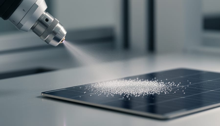
Which Solar Panel Components Can Be 3D Printed
Not every solar panel component benefits equally from additive manufacturing. The technology works best for specific parts where design flexibility or reduced material waste outweighs production speed.
Contact grids and busbars represent the most practical application today. Traditional screen printing wastes conductive silver paste and limits grid patterns to standardized geometries. 3D printing deposits metal precisely where needed, reducing material costs by 30-40% while enabling complex grid designs that minimize shading losses. Manufacturers can test new patterns without retooling entire production lines.
Encapsulation structures suit additive processes when custom shapes matter. Standard EVA lamination works fine for rectangular panels, but building-integrated applications need curved or angular encapsulants. Printing these eliminates expensive molds for low-volume runs.
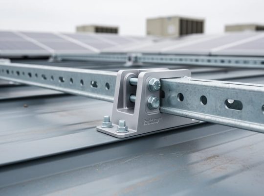
Mounting frames and junction boxes are straightforward candidates. Lightweight polymer frames printed on demand reduce warehousing costs and allow project-specific modifications. However, injection molding still wins for high-volume standard designs.
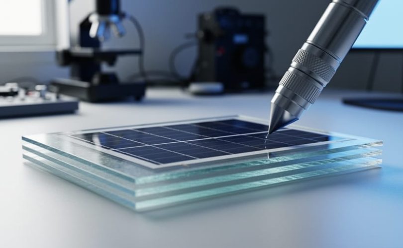
The real frontier lies in fully-printed cell prototypes. Researchers have demonstrated a 3D-printed solar cell using perovskite materials that achieves respectable conversion efficiencies. These aren’t replacing crystalline silicon cells yet, but they open doors for organic photovoltaics and tandem designs impossible to manufacture conventionally.
What can’t be printed effectively? Silicon wafers themselves. The crystalline growth and doping processes require specialized furnaces and semiconductor-grade precision that additive methods can’t match. Anti-reflective coatings also perform better when applied through chemical vapor deposition rather than printing.
The pattern holds: 3D printing excels where customization, material reduction, or novel geometries matter more than mass production speed.
Economic Advantages of Additive Manufacturing for Solar PV
Additive manufacturing fundamentally changes the economic equation for solar PV production by addressing three major cost drivers: material utilization, capital equipment requirements, and manufacturing flexibility. Traditional silicon solar cell production wastes approximately 40-50% of semiconductor material during sawing and processing, while 3D printing achieves near-zero waste by depositing material only where needed.
The capital expense difference proves equally significant. Conventional solar manufacturing lines require multi-million dollar investments in clean rooms, diffusion furnaces, screen printers, and lamination equipment. A 3D printing setup for specialized solar components can operate with entry costs 60-80% lower, making small-batch production and rapid prototyping financially viable for the first time. This democratizes innovation, allowing research institutions and startups to test novel designs without prohibitive upfront investment.
| Cost Factor | Traditional Manufacturing | 3D Printing |
|---|---|---|
| Material Waste | 40-50% silicon loss | 5-10% material loss |
| Tooling Investment | $2-5M for production line | $100K-500K for specialized printers |
| Labor Requirements | High skilled workforce for assembly | Automated deposition, minimal handling |
| Design Change Cost | Retooling required ($50K-200K) | Software update only |
Manufacturing flexibility delivers perhaps the most underappreciated economic benefit. Traditional production lines optimize for identical panels at massive scale; changing a busbar pattern or contact grid design requires expensive retooling and production downtime. With additive manufacturing, design modifications happen in software. A manufacturer can produce custom-shaped panels for architectural integration in the morning and standard rectangular modules in the afternoon without changing equipment or incurring setup costs.
Labor costs shift rather than disappear entirely. While 3D printing reduces assembly workers, it demands materials scientists and process engineers who understand deposition parameters and material properties. For manufacturers producing specialized panels or serving niche markets where customization commands premium pricing, these economics make compelling sense even at current efficiency levels.
Performance Considerations and Current Limitations
While additive manufacturing shows genuine promise for solar PV production, current performance metrics reveal substantial gaps compared to conventional silicon panels. Understanding these limitations helps manufacturers and industry professionals set realistic expectations and identify where the technology delivers actual value today.
Efficiency Remains the Primary Challenge
As of 2026, most 3D printed photovoltaic cells achieve conversion efficiencies between 8% and 15%, significantly below the 20-22% typical of mass-produced crystalline silicon modules. Printed perovskite cells have reached laboratory efficiencies approaching 18%, but translating these results to consistent production remains difficult. The layer-by-layer deposition process often introduces microscopic irregularities that create resistance losses and reduce overall electrical performance. Unlike traditional cell manufacturing where inline metrology catches defects before they propagate, additive processes currently lack real-time quality control at comparable sophistication levels.
Durability Questions for Real-World Deployment
Long-term stability testing reveals concerning degradation rates for many printable materials. Organic photovoltaics lose 20-30% of their initial output within the first year under outdoor conditions, while traditional panels typically degrade less than 1% annually. Moisture infiltration and UV exposure accelerate breakdown in polymer-based printed components. Encapsulation methods developed for silicon cells don’t always protect printed layers effectively, requiring specialized barrier materials that add complexity and cost.
Production Speed and Scale Constraints
Current 3D printing systems produce solar components at speeds measured in minutes per panel, versus seconds for conventional assembly lines. A single industrial printer might output 50 panels daily, compared to thousands from traditional manufacturing equipment. Material deposition rates limit throughput, and printer reliability issues cause production interruptions that would be unacceptable in high-volume operations.
Material Consistency and Supply Chain Issues
Photovoltaic inks and conductive pastes show batch-to-batch variations that affect performance predictability. The supply chain for specialized printing materials remains immature, with limited vendors and higher per-unit costs than bulk silicon feedstock. Quality standards for printable materials are still evolving, making procurement and performance validation more complex than sourcing traditional components.
Innovations in Printable Photovoltaic Cell Design

Perovskite solar cells have emerged as the most promising candidates for 3D printing, with their solution-processable nature allowing deposition at temperatures below 150°C. Unlike silicon cells requiring extreme heat and vacuum conditions, perovskites can be printed using inkjet or aerosol jet methods with remarkable precision. Laboratory prototypes now exceed 25% efficiency, closing the gap with traditional silicon while offering manufacturing flexibility silicon cannot match.
The key innovation lies in multi-layer printing strategies. Researchers deposit electron transport layers, perovskite absorbers, and hole transport layers sequentially without breaking vacuum or switching equipment. This integrated approach reduces contamination risks and production time. Recent work from Oxford PV and Saule Technologies demonstrates that printed perovskite-on-silicon tandem cells can surpass 29% efficiency, though these remain in pilot production rather than mass manufacturing.
Organic photovoltaics (OPVs) present different advantages. These carbon-based cells print onto flexible substrates using roll-to-roll processes similar to newspaper printing. While efficiency typically ranges between 12-15%, OPVs excel in low-light conditions and offer unprecedented form factor versatility. Their semi-transparency makes them particularly suitable for building-integrated applications where aesthetics matter as much as performance.
Hybrid designs combine materials to exploit complementary strengths. Printed quantum dot solar cells layered with organic materials achieve broader spectral absorption than either technology alone. Some research teams print conductive grids and anti-reflective nanostructures onto conventional cells, enhancing performance without replacing the entire manufacturing process.
The most significant recent development involves stabilizing printed perovskites against moisture and heat degradation. Encapsulation techniques using printed polymer barriers now extend operational lifetimes beyond 20 years in accelerated testing, addressing the primary concern holding back commercial deployment. However, few printed cells have undergone real-world field testing comparable to silicon’s decades of proven durability data.
Applications Where 3D Printed Solar Excels

While 3D printing hasn’t replaced conventional silicon PV modules for utility-scale installations, it delivers compelling advantages in specialized applications where traditional manufacturing falls short. The technology’s strength lies in customization, rapid iteration, and economically viable small-batch production.
Building-Integrated Photovoltaics (BIPV) represents the most promising commercial application for additive manufacturing. Architects designing energy-generating facades require panels shaped to fit specific curves, angles, and aesthetic requirements that standard rectangular modules cannot accommodate. Traditional manufacturing demands expensive custom tooling for each unique shape, making bespoke designs economically prohibitive. 3D printing eliminates tooling costs entirely, allowing manufacturers to produce architecturally tailored solar components at reasonable prices for projects ranging from curved building facades to solar-integrated window frames.
Rapid prototyping dramatically accelerates development cycles for researchers and manufacturers testing new cell configurations. A 3D digital twin combined with additive manufacturing enables teams to move from design concept to physical prototype within days rather than the months required for conventional fabrication. This speed proves invaluable when evaluating contact grid patterns, testing new materials, or validating performance assumptions before committing to large-scale production.
The technology excels in several other scenarios where conventional manufacturing proves impractical:
- Remote or off-grid applications requiring lightweight, portable solar solutions that can be printed on-site
- Small satellites and aerospace applications demanding custom-fitted panels with minimal mass
- Replacement components for discontinued panel models where original tooling no longer exists
- Educational and research institutions producing small quantities of experimental cell designs
- Consumer electronics requiring solar integration in unconventional form factors
These niche applications collectively represent significant market opportunities. As material costs decline and printing speeds improve, the economic threshold where additive manufacturing becomes viable will expand to include larger production volumes and additional use cases.
Integration with Traditional Solar Manufacturing
Rather than displacing established silicon photovoltaic manufacturing, 3D printing is finding its most practical applications as a complementary technology that addresses specific production challenges. Traditional crystalline silicon cell fabrication, with its proven efficiency above 22% and decades of refinement, remains the foundation of commercial solar production. Additive manufacturing enhances this foundation by targeting components where conventional methods create bottlenecks or waste.
The most commercially viable hybrid approach involves printing contact grids and busbars onto traditionally manufactured silicon wafers. Screen printing pastes for front contacts waste significant quantities of expensive silver while limiting design flexibility. Aerosol jet printing deposits conductive materials with precision that reduces silver consumption by 40-60% and enables finer grid patterns that improve light capture. Manufacturers integrate these printing systems into existing production lines between wafer preparation and lamination stages.
Another productive integration point appears in encapsulation and edge sealing. Traditional EVA lamination works well for standard rectangular modules, but custom shapes and building-integrated applications require adaptable encapsulation methods. Selective dispensing of printable encapsulants allows manufacturers to produce non-standard geometries without expensive custom tooling, opening architectural markets that conventional lines cannot serve economically.
For prototyping new cell designs, 3D printing accelerates development cycles dramatically. Engineers can print test structures, junction layers, or anti-reflection coatings in hours rather than waiting weeks for photolithography mask fabrication. Once validated through printed prototypes, successful designs transition to high-volume conventional production.
This hybrid model lets manufacturers leverage their substantial investments in silicon processing infrastructure while gaining flexibility, reducing material costs, and accessing specialized markets that pure traditional methods cannot reach profitably.
What Aspiring PV Professionals Need to Know
As additive manufacturing reshapes solar production, professionals entering the PV sector need a broader skill set than previous generations. Traditional solar manufacturing expertise remains foundational, but proficiency in digital design tools, especially CAD software for component modeling, has become essential for those working with or around 3D printing processes.
Materials science knowledge takes on new importance when working with printable photovoltaics. Understanding how conductive inks behave during deposition, how polymer substrates interact with semiconductor materials, and how printed layers cure and bond differs fundamentally from conventional silicon wafer processing. Professionals who can bridge traditional PV knowledge with additive manufacturing principles will find themselves uniquely positioned as hybrid production approaches gain traction.
Process optimization skills matter increasingly as well. The ability to work with digital twins and simulation software helps predict how design changes affect both printability and electrical performance before physical prototyping begins. This computational approach reduces development costs and accelerates innovation cycles.
Quality assurance protocols for 3D printed components require different testing methodologies than those used for conventional panels. Aspiring professionals should familiarize themselves with non-destructive testing techniques, layer adhesion analysis, and performance validation methods specific to additive manufacturing.
The most valuable professionals will be those who understand where 3D printing complements traditional methods rather than viewing technologies as competing alternatives. This systems-level perspective, combined with practical skills in both domains, positions individuals to contribute meaningfully as the industry adopts hybrid manufacturing approaches over the coming years.
3D printing in solar panel manufacturing currently occupies a specialized niche rather than mainstream production. The technology demonstrates clear advantages in prototyping, custom applications, and specific component manufacturing, but it has not replaced traditional silicon cell production methods. Most commercial deployments combine additive manufacturing for select components with conventional processes for core photovoltaic elements.
Realistic adoption timelines vary significantly by application. Printed contact grids and busbars are seeing commercial implementation now in 2026, with several manufacturers integrating these into production lines. Fully printed perovskite modules remain primarily in research phases, with commercial viability expected within three to five years for niche applications. Widespread adoption of entirely 3D printed solar panels for utility-scale installations likely sits beyond a ten-year horizon, contingent on resolving durability and efficiency challenges.
The technology will function as a complement to traditional manufacturing rather than a replacement. Hybrid approaches leveraging strengths of both methods appear most promising. Additive manufacturing excels at customization, rapid iteration, and reducing material waste for specific components, while conventional methods maintain superiority in high-volume production of standardized silicon cells.
For industry stakeholders, the opportunity lies in strategic integration. Manufacturers can adopt 3D printing selectively where it provides economic or technical advantages without abandoning proven production methods. For professionals entering photovoltaic fields, familiarity with both traditional and additive processes creates competitive advantage. The convergence of materials science, digital design capabilities, and manufacturing engineering defines the skillset for next-generation solar production specialists.
Mose Solar’s university collaborations and educational programs prepare professionals to navigate this evolving landscape, equipping them with knowledge spanning conventional and emerging manufacturing technologies that will shape the industry’s future.