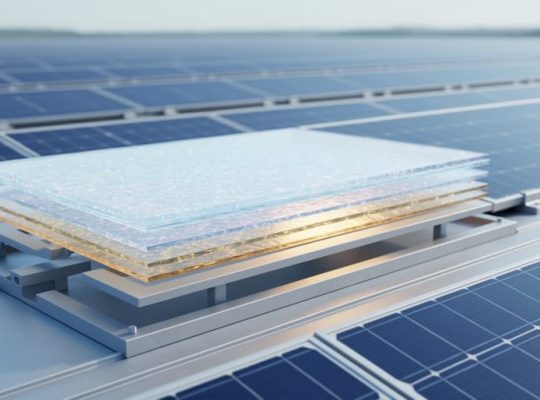
First Solar’s manufacturing process represents a fundamental departure from conventional silicon photovoltaic production, relying instead on cadmium telluride (CdTe) thin-film technology deposited on glass substrates through vapor transport deposition. This continuous, automated process builds complete solar modules in a single production line, achieving material efficiencies and cost advantages that traditional crystalline silicon manufacturing cannot match. Rather than sawing ingots or assembling discrete cells, First Solar’s approach deposits semiconductor layers just a few micrometers thick onto large glass sheets, integrating scribing, electrical interconnection, and encapsulation within a streamlined workflow.
The distinction matters because CdTe thin-film manufacturing requires substantially less energy, lower capital expenditure per watt, and shorter production cycles than multicrystalline or monocrystalline silicon facilities. Where silicon manufacturing demands high-temperature furnaces, extensive material handling, and multi-stage cell assembly, First Solar’s process operates at lower temperatures and completes module fabrication in approximately 2.5 hours from raw glass to finished product. This efficiency has positioned the company as a leader in U.S. solar manufacturing with production capacity exceeding 10 gigawatts annually as of 2026.
Understanding this process is essential for photovoltaic professionals evaluating manufacturing pathways, researchers exploring alternative semiconductor technologies, and industry stakeholders assessing competitive positioning in utility-scale solar markets. The technical and operational requirements differ markedly from silicon-based facilities, demanding specialized knowledge in vapor deposition chemistry, semiconductor physics, and high-throughput automation systems that this article will systematically address.
What Is the First Solar Manufacturing Process?
The Thin-Film Cadmium Telluride Technology
Cadmium telluride operates as a direct bandgap semiconductor with an optimal energy gap of approximately 1.45 electron volts, closely matching the solar spectrum’s peak intensity. This property allows CdTe to absorb sunlight efficiently within an extremely thin layer, typically just 2-8 micrometers thick, compared to the 180-200 micrometer thickness required for crystalline silicon wafers. The absorption coefficient of CdTe exceeds 10^5 cm^-1 for photons above its bandgap energy, meaning it captures over 90% of usable sunlight in a film thinner than a human hair.
This exceptional light absorption translates directly into manufacturing advantages. While silicon wafer production requires energy-intensive processes including polysilicon purification at 1,414°C and crystal growth in Czochralski furnaces, CdTe deposition occurs at temperatures between 500-600°C. The lower thermal budget reduces energy consumption per module by approximately 40-50% compared to multicrystalline silicon manufacturing.
The direct bandgap structure also eliminates the need for thick material to achieve adequate photon capture. Silicon’s indirect bandgap requires photons to interact with lattice vibrations (phonons) for electron excitation, necessitating longer optical path lengths through thicker material. CdTe’s direct transition allows immediate electron-hole pair generation upon photon absorption, achieving comparable quantum efficiency with far less semiconductor material.
Manufacturing speed benefits significantly from these properties. First Solar’s vapor transport deposition process deposits CdTe layers in minutes rather than the hours required for silicon ingot growth and sawing. The reduction in material thickness, processing temperature, and deposition time creates a manufacturing cycle measured in hours from substrate to finished module, compared to days for conventional silicon production. This temporal efficiency, combined with lower capital equipment costs for thin-film deposition systems versus silicon crystal pullers, establishes CdTe as a fundamentally different manufacturing paradigm.
Vapor Transport Deposition and Layer Assembly
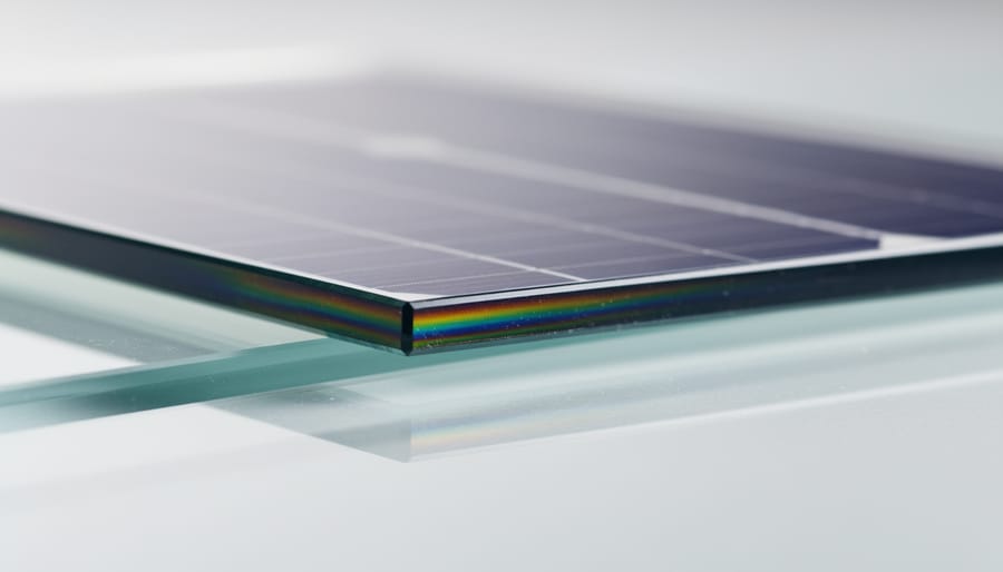
The vapor transport deposition (VTD) process begins with rigorous substrate preparation. Large glass sheets, typically soda-lime float glass measuring approximately 60 cm by 120 cm, undergo chemical cleaning to remove surface contaminants and organic residues that could compromise layer adhesion. The glass is then preheated to controlled temperatures, ensuring uniform thermal conditions before the deposition chambers receive it.
Inside the deposition system, the cleaned glass substrate moves through sequential chambers, each engineered to deposit a specific semiconductor layer. The first deposition step applies a transparent conducting oxide (TCO) layer, usually cadmium stannate or tin oxide, which functions as the front electrical contact. This layer must balance high electrical conductivity with maximum light transmission to enable photons to reach the active semiconductor layers beneath.
The critical CdTe absorber layer follows next through VTD deposition on glass where heated cadmium and tellurium sources vaporize the materials at precisely controlled temperatures between 550°C and 650°C. The vapor molecules travel across a controlled gap and condense onto the moving glass substrate, forming a uniform polycrystalline film typically 2 to 8 microns thick. Deposition rates, substrate temperature, and vapor pressure require continuous monitoring to achieve the correct crystal structure and grain boundaries that determine the final module’s conversion efficiency.
A thin cadmium sulfide (CdS) layer deposits before the CdTe absorber, creating the crucial p-n junction where charge separation occurs. This window layer measures only 50 to 150 nanometers, requiring extreme precision. The interface between CdS and CdTe defines the device’s electronic properties, so process engineers maintain strict tolerances on thickness uniformity, deposition rate, and chamber atmosphere composition.
Following semiconductor deposition, a back contact layer, typically a carbon-based composite with metallic components, completes the electrical circuit. Each layer transition happens within controlled atmospheres, often under vacuum or inert gas environments, preventing oxidation and contamination. Real-time thickness monitors and optical sensors verify that each layer meets specification before the substrate advances, ensuring high production yields and consistent module performance.
Manufacturing Requirements and Technical Specifications

Facility and Equipment Prerequisites
Establishing a First Solar, style CdTe production facility demands substantial infrastructure distinct from silicon wafer plants. Manufacturing plants require ISO Class 6 to Class 7 cleanrooms (10,000 to 100,000 particles per cubic foot) to prevent contamination during vapor deposition, with temperature and humidity controls maintaining 68-72°F and 40-50% relative humidity throughout production zones. These environmental standards protect semiconductor layer integrity during the critical deposition phases.
Vapor transport deposition chambers form the technological core, operating at 550-650°C to sublimate cadmium and tellurium compounds onto glass substrates. Each chamber typically measures 15-20 feet in length and processes substrates moving at controlled speeds of 1-3 meters per minute. Modern facilities employ parallel deposition lines with 8-12 chambers per line, enabling annual production capacities exceeding 1 gigawatt.
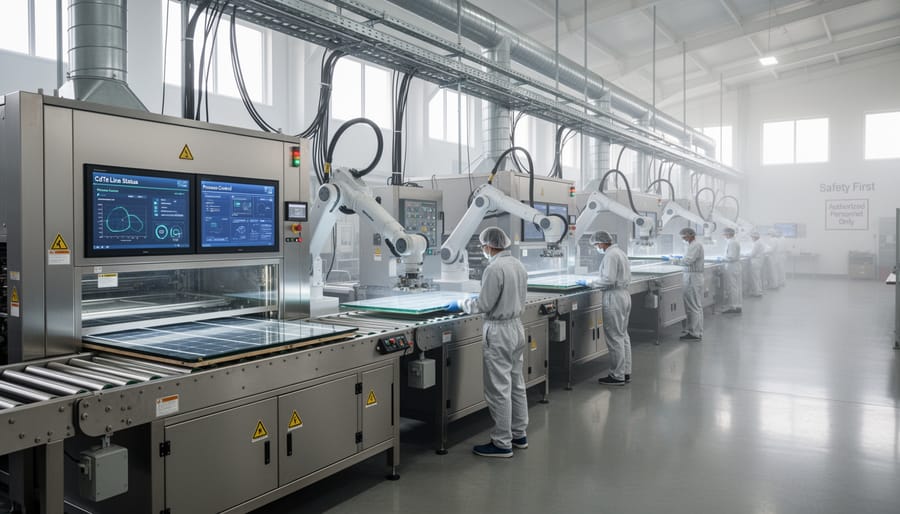
Automated handling systems transport glass substrates between deposition stages, applying protective coatings, and routing modules through inspection stations without manual intervention. Robotic transfer mechanisms prevent substrate damage while maintaining cleanroom integrity. Testing equipment includes electroluminescence imaging systems that detect microcracks and electrical discontinuities, flash testers measuring power output under standard test conditions, and environmental chambers simulating temperature cycling and humidity exposure.
Capital requirements for a complete facility exceed $150 million, reflecting the specialized nature of thin-film manufacturing equipment and the cleanroom infrastructure essential for consistent production yields. This significant solar investment explains why only vertically integrated manufacturers have successfully implemented CdTe production at commercial scale.
Material Supply and Quality Standards
First Solar’s CdTe manufacturing demands precise material specifications beginning with ultra-pure cadmium (99.9999% purity) and tellurium (99.999% purity) to ensure optimal semiconductor performance. Unlike silicon production requiring polysilicon refining, CdTe processing uses these elements in powder or vapor form, sourced primarily from zinc mining by-products and copper refining operations. Supply contracts must guarantee consistent chemical composition because trace impurities directly affect absorption efficiency and long-term degradation rates.
Glass substrates require low-iron soda-lime composition with transmission rates exceeding 91% across the solar spectrum. Thickness tolerance holds to ±0.2mm, and surface flatness must stay within 0.5mm deviation across a 1.2m × 0.6m panel to prevent deposition irregularities. The glass supplier qualifies through accelerated weathering tests simulating 25-year outdoor exposure, with rejection criteria set at any hazing, delamination or transmission loss beyond 2%.
Encapsulation materials, typically ethylene vinyl acetate (EVA) or polyvinyl butyral (PVB), undergo moisture vapor transmission rate testing (must remain below 0.1 g/m²/day) and UV stability verification. Back-sheet laminates require passing 1,000-hour damp-heat exposure at 85°C/85% relative humidity without adhesion failure.
Quality protocols mandate incoming material certification, statistical process control during deposition, and batch testing for every production shift. Non-conforming materials trigger immediate line stoppage, with root-cause analysis required before resuming operations. This rigor keeps module efficiency variance within ±3% across production runs.
Implementing the Manufacturing Process: Steps and Protocols
Production Line Configuration
Establishing an automated First Solar production line requires configuring several integrated systems that work in continuous sequence. The foundation involves positioning vapor deposition chambers in a linear arrangement that allows glass substrates to progress through each semiconductor layer application without human handling. These chambers must maintain precise temperature zones, typically between 500-600°C for CdTe deposition, with automated feedback controls adjusting vapor flow rates to ensure uniform layer thickness across each 0.6 × 1.2-meter glass panel.
Material handling systems use robotic transfer mechanisms with vacuum grippers designed specifically for thin glass substrates, moving panels between deposition stages at controlled speeds that prevent thermal shock. Inline metrology stations positioned after each major deposition step measure layer thickness using optical sensors, immediately flagging panels that fall outside specification tolerances before they proceed further down the line.
Quality inspection integration occurs at strategic checkpoints: substrate cleaning verification uses automated optical inspection before deposition begins, while post-encapsulation stations perform preliminary electrical testing to identify shorts or open circuits. Modern facilities increasingly incorporate digital innovation through real-time production monitoring dashboards that track yield metrics, chamber performance parameters, and maintenance schedules across all deposition systems simultaneously.
Continuous flow depends on buffer zones between processing stages, typically holding 15-20 panels, that absorb minor timing variations without halting upstream equipment. Configuring these buffers correctly prevents bottlenecks while maintaining the steady throughput essential for achieving First Solar’s target production rates of one panel every 15-20 seconds.
Quality Control and Testing Protocols
First Solar’s quality assurance framework validates every module through a multi-stage testing sequence before commercial release. Electroluminescence imaging scans completed panels for microcracks, inactive cell regions, or electrical inconsistencies invisible to visual inspection, ensuring structural integrity across the semiconductor layers. Flash testing follows, where calibrated light pulses simulate standard solar conditions (1000 W/m² irradiance, 25°C cell temperature) to measure actual power output, voltage-current characteristics, and efficiency ratings against nameplate specifications, modules failing to meet minimum performance thresholds get rerouted for analysis or reprocessing.
Environmental stress testing subjects sample batches to accelerated aging protocols: thermal cycling between -40°C and 85°C, damp heat exposure at 85°C and 85% relative humidity for 1,000 hours, and mechanical load simulations replicating wind, snow, and mounting stresses. These IEC 61646 certification tests predict 25-year field performance and identify potential degradation pathways specific to thin-film technology. Advanced facilities now integrate digital transformation tools, machine learning algorithms analyze testing data to detect subtle patterns predicting long-term reliability, while automated optical inspection stations photograph every module for traceability. UL certification, CE marking for European markets, and utility-scale bankability assessments round out compliance requirements, with independent third-party laboratories periodically auditing production samples to verify manufacturing consistency meets international standards.
Operational Responsibilities and Environmental Compliance
Cadmium Management and Safety Protocols
Cadmium management in CdTe manufacturing facilities operates under strict federal and state regulations administered by OSHA and EPA. The permissible exposure limit for airborne cadmium stands at 5 micrograms per cubic meter as an eight-hour time-weighted average, with action levels triggering mandatory medical surveillance when workers face half that concentration. First Solar and similar manufacturers implement closed-loop vapor deposition systems that prevent cadmium release during production, combining negative-pressure cleanrooms with HEPA filtration and continuous air monitoring to maintain concentrations well below regulatory thresholds.
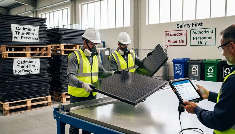
Worker protection protocols require respiratory protection for maintenance operations, quarterly biological monitoring through urine cadmium testing, and comprehensive training on cadmium toxicity and safe handling procedures. Facilities maintain dedicated decontamination zones where workers remove protective equipment and shower before exiting production areas. Emergency response plans address potential vapor release scenarios with automated shutdown systems, area evacuation procedures, and specialized spill containment materials.
Regulatory compliance extends beyond manufacturing floors to align with broader solar policies governing hazardous material use in renewable energy production. Manufacturers submit annual toxic release inventory reports and maintain financial assurance mechanisms for facility closure, ensuring responsible decommissioning when production ceases.
End-of-Life Module Collection and Recycling
First Solar operates one of the solar industry’s most comprehensive module recycling programs, establishing manufacturer responsibility that extends decades beyond installation. The company commits to collecting and recycling modules at end of life, typically 25-30 years after deployment, with this obligation embedded in product warranties and formalized through prepaid recycling programs that fund future collection costs.
The recycling infrastructure centers on specialized processing facilities capable of recovering over 90% of semiconductor materials and glass substrates from retired modules. Modules undergo systematic disassembly where aluminum frames and junction boxes are separated first, followed by semiconductor layer recovery through proprietary extraction techniques. The cadmium and tellurium semiconductor materials are chemically separated from glass substrates, purified to manufacturing-grade quality, then reintroduced into production lines for new module fabrication.
Glass represents the largest recoverable component by mass, with crushed cullet meeting specifications for new solar glass or construction materials. This closed-loop material flow reduces primary mining requirements for tellurium and cadmium while eliminating landfill disposal concerns that critics historically raised about CdTe technology.
Manufacturers implementing similar thin-film processes must establish financial assurance mechanisms, documented collection logistics across operational territories, and processing partnerships that guarantee material recovery rather than disposal. First Solar’s model demonstrates how proactive end-of-life management addresses regulatory requirements while creating economic value from material reclamation.
Technical Support and Industry Resources
Professionals implementing or researching thin-film CdTe manufacturing can access a range of technical resources, regulatory guidance, and educational programs that support technology transfer and workforce development in this specialized field.
First Solar maintains a technical support portal for manufacturing partners and research collaborators, offering process documentation, equipment specifications, and quality assurance guidelines. The company’s published patents and peer-reviewed research papers provide detailed insights into vapor transport deposition techniques and module design innovations. Manufacturing engineers can consult First Solar’s sustainability reports for environmental compliance frameworks specific to cadmium management and recycling operations.
University research partnerships have accelerated advances in thin-film manufacturing science. The National Renewable Energy Laboratory (NREL) maintains an extensive database of CdTe cell efficiency records, material characterization data, and manufacturing process models. Colorado State University’s Next Generation Photovoltaics Center conducts fundamental research on semiconductor deposition methods, while Ohio State University collaborates with industry partners on manufacturing automation and quality control systems. These academic institutions offer specialized coursework and laboratory training for graduate students pursuing careers in photovoltaic manufacturing.
Key technical and educational resources include:
- First Solar Technical Documentation Portal, process specifications, equipment requirements, and quality standards
- National Renewable Energy Laboratory (NREL), CdTe research database, manufacturing models, and efficiency tracking
- SEMI Photovoltaic Standards, industry specifications for equipment, materials, and testing protocols
- Environmental Protection Agency (EPA), cadmium handling regulations and disposal requirements
- Solar Energy Industries Association (SEIA), manufacturing workforce development programs and policy guidance
Regulatory agencies provide essential compliance guidance. The EPA’s Resource Conservation and Recovery Act (RCRA) program outlines cadmium waste management requirements, while OSHA standards specify workplace exposure limits and safety protocols for semiconductor manufacturing environments.
Mose Solar actively collaborates with academic institutions to develop curriculum and hands-on training programs that prepare aspiring PV professionals for careers in advanced solar manufacturing. These educational partnerships combine theoretical understanding of thin-film physics with practical experience in cleanroom protocols, vapor deposition techniques, and quality assurance methodologies. Certificate programs and internship placements connect students with manufacturing facilities seeking skilled technicians and process engineers. Trade associations such as SEIA and the International Renewable Energy Agency (IRENA) offer continuing education courses on emerging manufacturing technologies and industry best practices.
Who Qualifies and What You Need
Implementing First Solar’s thin-film CdTe manufacturing process requires substantial capital investment, technical expertise, and regulatory compliance rather than traditional eligibility screening. Organizations pursuing this technology typically need $200-500 million in initial capital for facility construction, equipment procurement, and production line setup. Manufacturing partners must demonstrate proven experience in precision industrial processes, cleanroom operations, or semiconductor fabrication.
Technical qualifications include engineering teams with expertise in vapor deposition systems, automated material handling, and quality assurance protocols. Facilities require appropriate zoning for industrial manufacturing and environmental permits addressing cadmium handling, air quality management, and waste disposal systems. You’ll need comprehensive safety documentation covering worker protection protocols, emergency response plans, and hazardous material management procedures that meet OSHA standards and EPA regulations.
Licensing agreements with First Solar or comparable thin-film technology providers demand intellectual property compliance and adherence to proprietary process specifications. Material suppliers must meet strict purity standards for cadmium, tellurium, and glass substrates, supported by certified quality documentation and chain-of-custody records. Organizations entering this manufacturing space should prepare detailed business plans demonstrating technical capability, financial stability, and long-term commitment to environmental stewardship throughout the product lifecycle.
Where to Get Official Help
Professionals seeking technical guidance on thin-film manufacturing should contact First Solar’s Technology Partnership Program directly through their corporate headquarters in Tempe, Arizona, or regional offices in Ohio, Malaysia, and Vietnam. The company maintains dedicated technical support channels for manufacturing inquiries, research collaborations, and process licensing discussions.
For regulatory compliance questions regarding cadmium handling and CdTe production, consult the Environmental Protection Agency’s Industrial Photovoltaic Manufacturing Division and OSHA’s Semiconductor Manufacturing Safety Guidelines. State environmental agencies provide jurisdiction-specific permitting requirements for thin-film facilities.
Academic researchers and aspiring PV professionals can access manufacturing education through SEIA’s Manufacturing Training Initiative and university partnerships. Mose Solar collaborates with leading photovoltaic engineering programs to provide hands-on training in both thin-film and crystalline silicon production techniques, including modules on integrated solar storage systems that complement advanced manufacturing knowledge.
The National Renewable Energy Laboratory (NREL) offers process research data, efficiency benchmarking studies, and manufacturing cost analyses through their publicly accessible technical reports database, essential references for understanding thin-film production economics and performance metrics.
Common Questions About First Solar’s Manufacturing Process
How does CdTe efficiency compare to crystalline silicon modules?
First Solar’s CdTe modules typically achieve 18-19% efficiency in commercial production, while premium monocrystalline silicon panels reach 21-23%. However, CdTe’s superior temperature coefficient and lower degradation rates often result in comparable energy yields over the module’s lifetime, particularly in hot climates where silicon efficiency drops significantly.
What manufacturing cost advantages does the CdTe process offer?
The vapor transport deposition process requires substantially less energy than silicon wafer production, operates at lower temperatures (around 600°C versus 1400°C for silicon), and uses 1-2% of the semiconductor material needed for crystalline modules. These factors combine to produce manufacturing costs approximately 30-40% lower per watt of capacity.
Is cadmium in CdTe modules a safety concern?
The cadmium telluride compound is chemically stable and encapsulated within glass layers, making it safe during normal operation and even in fire scenarios. First Solar’s comprehensive recycling program recovers over 90% of cadmium from retired modules, preventing environmental release and ensuring responsible end-of-life management.
Can the CdTe manufacturing process scale to meet growing demand?
First Solar has demonstrated scalability by operating gigawatt-scale facilities with highly automated production lines that can manufacture a module every few seconds. The primary scaling constraint involves tellurium availability, though current production levels represent a small fraction of global tellurium supply from copper refining byproducts.
Beyond these core questions, professionals evaluating CdTe technology often ask about performance degradation patterns. First Solar modules exhibit minimal light-induced degradation compared to silicon’s initial power loss, maintaining stable output after a brief stabilization period. The modules also demonstrate exceptional resilience in humidity and salt-mist environments, making them particularly suitable for coastal installations and desert utility-scale projects.
The competitive positioning of CdTe manufacturing centers on total cost of ownership rather than peak efficiency metrics. While crystalline silicon dominates residential rooftop markets where space constraints prioritize high efficiency, CdTe’s lower balance-of-system costs and superior real-world energy production make it economically attractive for utility-scale ground-mounted arrays where land availability is less restrictive.
Future process improvements focus on increasing active area utilization, reducing manufacturing cycle times through enhanced deposition rates, and incorporating bifacial designs that capture reflected light from the ground. Research partnerships between manufacturers and universities continue exploring alternative transparent conducting oxides and advanced encapsulation materials that could push efficiency beyond 20% while maintaining the inherent manufacturing cost advantages that define the technology.
First Solar’s manufacturing process represents a critical alternative pathway in photovoltaic production, demonstrating that thin-film CdTe technology can compete with traditional crystalline silicon through vertically integrated operations and automated efficiency. This diversity in manufacturing approaches strengthens the solar industry’s resilience, offering distinct advantages in specific deployment scenarios where low-temperature coefficients, reduced embodied energy, and rapid production cycles provide value. For jurisdictions seeking domestic manufacturing capacity or projects requiring particular performance characteristics, understanding multiple production methodologies expands strategic options.
Professionals entering the photovoltaic sector benefit from recognizing that solar manufacturing encompasses varied technical disciplines beyond silicon wafer processing. Expertise in vapor deposition techniques, thin-film semiconductor physics, and closed-loop recycling systems creates specialized career pathways within renewable energy. Mose Solar’s educational programs address this diversity by partnering with universities to train aspiring professionals across multiple manufacturing platforms, ensuring graduates possess both theoretical understanding and practical knowledge of evolving production technologies.
The continued refinement of First Solar’s process, alongside advancements in silicon-based manufacturing and emerging technologies, signals an industry maturing toward optimized solutions rather than single dominant approaches. This technical plurality drives innovation, cost reduction, and performance improvements that accelerate global solar adoption.